
Semiconductors fuel today’s electronics. They start with raw materials that decide how well they work, how much they cost, and how much they can grow. These materials are super important in Semiconductor manufacturing and help run our modern tech world. Stuff like silicon (Si), germanium (Ge), gallium arsenide (GaAs), phosphorus (P), boron, and gallium has replaced old heat-based devices. These bits allow quick data work, good energy use, and tiny designs.
Why Are Semiconductor Materials So Important to the World’s Economy?
What Do Raw Materials Do in Semiconductor Manufacturing?
Semiconductors are the heart of electronics. Their making relies on raw materials that set quality, cost, and growth limits. These materials are a big deal in the Semiconductor manufacturing process. They make our tech world possible. By using things like silicon, germanium, gallium arsenide, phosphorus, boron, and gallium, old heat devices are gone. These materials help with fast data movement, smooth energy shifts, and small designs.
Silicon wafers are the base for building circuits. Silicon is the top material for making wafers. It’s key in chip production. Adding stuff like boron or phosphorus tweaks electrical features. Also, compound semiconductors like gallium arsenide and indium phosphide are must-haves for fast and light-based uses.
How Does Getting Materials Affect World Stability?
Semiconductor materials matter a lot globally. Germanium mostly comes from coal ash or zinc processing leftovers. The EU Critical Raw Materials Act (CRMA) says China leads in germanium production. It has 60% of the world’s share and sent out 43.7 tons in 2022. Gallium production is also mostly in East Asia. This one-area focus makes global supply chains shaky.
Some key elements, like indium and bismuth, are super rare in the Earth’s crust. Bismuth and indium are the rarest and most likely to run out. Any hiccups or export bans can mess up industries that need these materials.
Where Are Supply Chain Problems the Worst?
Supply chain risks come from focusing on one area and tricky processes. Many rare earths for doping or compound semiconductors come from places with political issues. Refining these materials needs special setups. These are tough to build in other places.
To cut risks, smart plans are needed. You can spread out suppliers, build local factories, or keep extra stock. This stops delays that could shut down whole Semiconductor plants.
Which Materials Are Speeding Up New Ideas?
Why Are Silicon Wafers Still the Main Choice Despite New Options?
Silicon stays on top because it’s common and has a solid production setup. It’s the second most common element (28%) in the Earth’s crust. So, silicon supply is pretty safe for now. Better monocrystalline silicon methods have made bigger wafers (300mm or more) with fewer mistakes.
But going below 5nm nodes needs super clean bases with almost no flaws or dirt. This pushes new ideas not just in silicon but also in how it works with other materials during layering and etching.
Why Are Compound Semiconductors Like GaN and SiC So Exciting?
Gallium nitride (GaN) and silicon carbide (SiC) do better than silicon in high-power or high-speed cases. Semiconductor wafers with gallium arsenide can take more heat and run faster than silicon ones. These features make them great for power parts in electric cars (EVs) or radio-frequency (RF) devices in 5G networks.

Indium phosphide is also a big player. It helps make laser beams and build quantum light circuits. Its direct bandgap lets it send out light well for lasers in fiber optics. These compound semiconductors are opening new paths in the telecom and energy areas.
How Is Material Purity Changing Manufacturing?
Why Is Super High Purity So Important Now?
As chips get smaller than 5nm, even tiny bits of dirt can wreck yields or reliability. The need for super-small chips makes ultra-pure chemicals—like sulfuric acid or hydrogen peroxide—and special gases crucial for etching and cleaning.
Purity affects mistakes during photolithography or doping. High-purity dopants like boron improve dielectric strength and keep dirt low. Boron makes insulating layers in chips work better.
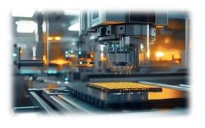
What Happens When You Go Below 5nm Nodes?
At these small sizes, EUV lithography is normal. But it brings new issues with material matches for photoresists and etch chemicals. Every layer—from hard masks to connections—must handle repeated patterning without breaking.
3D shapes like FinFETs or gate-all-around transistors make things harder. Etching precision is super important. This is where DEEPETCH stands out. Their flexible plasma etching platforms handle mixed dry and wet processes. They’re perfect for dealing with multi-material stacks with tiny-scale accuracy.
Can We Be Green Without Losing Performance?
What Green Issues Come with Rare Earths?
Mining rare earths often makes toxic waste and uses tons of energy. As world green rules get tougher, how we get materials is being watched closely. Not just by governments but also by investors who care about ESG goals.
Some think we should look at asteroid resources or use more common Semiconductor materials. But swapping out rare stuff like indium or gallium arsenide isn’t always doable. Their special electronic features are hard to replace.
How Is Recycling Part of Material Plans?
Recycling now targets packaging bases and reused silicon wafers after testing. Wafer reclaim processes cut waste while keeping a good enough surface quality for test uses or MEMS devices.
This reuse method is vital with material shortage risks. It also helps keep costs down while meeting rules for cutting carbon footprints.
Which Areas Lead—and Which Are Catching Up Quick?
Why Does Asia-Pacific Still Lead Global Production?
Asia-Pacific is ahead because of its tight-knit systems in Japan, South Korea, Taiwan, and China. These places shine in specialty chemicals and wafers. They focus on wafer making, advanced photoresists, and ultra-pure gases needed for top nodes.
These countries gain from years of spending on R&D centers near factories. This Amend
How Are North America and Europe Fighting Back?
Recent problems, like pandemics or geopolitical conflicts, have pushed Western countries to boost local material production. They use tax breaks and funding to build local factories.
The goal is simple: rely less on one region’s supply chains. They want strong systems covering mining to final chip packaging, ideally inside their borders.
How Do Specialty Chemical Suppliers Help Advanced Chips?
Why Do New Chips Need Custom Chemical Mixes?
As chip designs move from flat CMOS to stacked memory, special chemical blends are needed. These blends meet unique needs for selectivity, volatility, or heat stability during layering and etching.
This customization needs close teamwork between chip makers and chemical suppliers during R&D, not just mass production. It fine-tunes processes across different tools.
What Teamwork Models Push New Ideas Today?
Joint development agreements (JDAs) now cover chemistry development, not just factory-tool deals. Suppliers who plan early with you give an advantage. They ensure new materials fit smoothly into your workflows without costly delays.
Companies like DEEPETCH lead by offering modular etch systems that work with many chemistries. This lets you adapt fast as design rules change, keeping process stability and output high.
Where Is the Industry Going for Strength and Tech Leadership?
Should You Stockpile or Use Just-In-Time Logistics?
Stockpiling guards against disruptions but ties up money if not done right. A mixed plan works best. Keep reserves of risky materials. Use real-time data for stable ones like silicon wafers, which are less likely to run out.
Silicon makes up 28% of the Earth’s crust. It’s less risky than rare compounds like indium phosphide or bismuth-based dopants. Those need tighter stock control due to supply issues.
What New Ideas Are Coming in Etching for Advanced Nodes?
Dry etching is improving with better control for high-aspect-ratio tasks using atomic-layer precision. Wet etching is still cost-effective for some isotropic removal steps. Mixing both allows tailored processes per layer type. Hybrid tools like those from DEEPETCH offer this flexibility.
FAQ
Q1: Which raw material is most critical yet most at risk?
A: Indium is one of the rarest elements used in optoelectronics. Its short supply raises big concerns for long-term sustainability if no substitutes are found soon.
Q2: Why can’t we fully replace compound semiconductors with silicon?
A: Compound semiconductors work better in high-speed or high-heat settings where silicon struggles. Swapping them would hurt device efficiency.
Q3: How does DEEPETCH help manufacturers with advanced node challenges?
A: DEEPETCH provides flexible plasma etch platforms that work with both dry and wet methods. This is key below 5nm, where precision across multiple material layers is critical.


