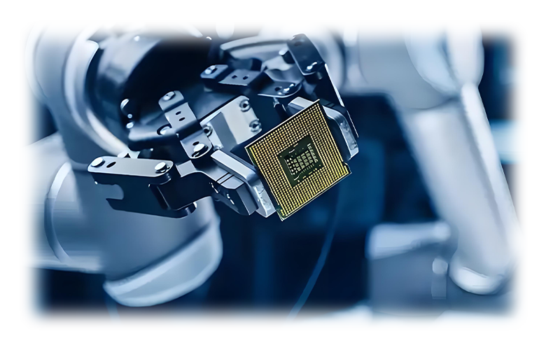
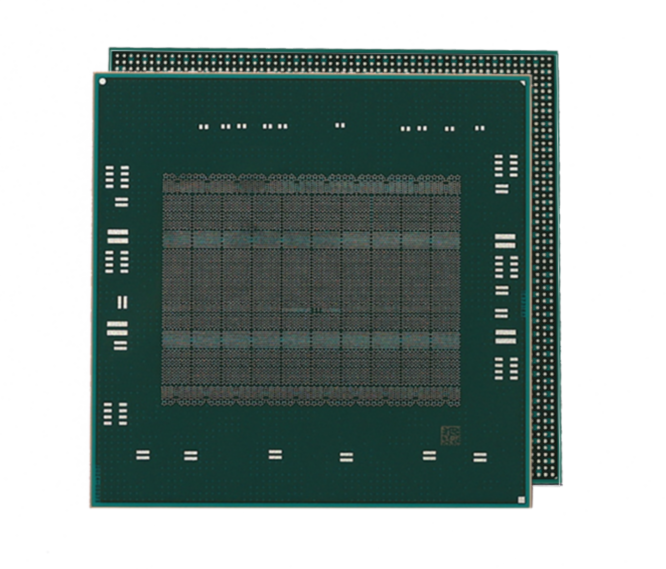
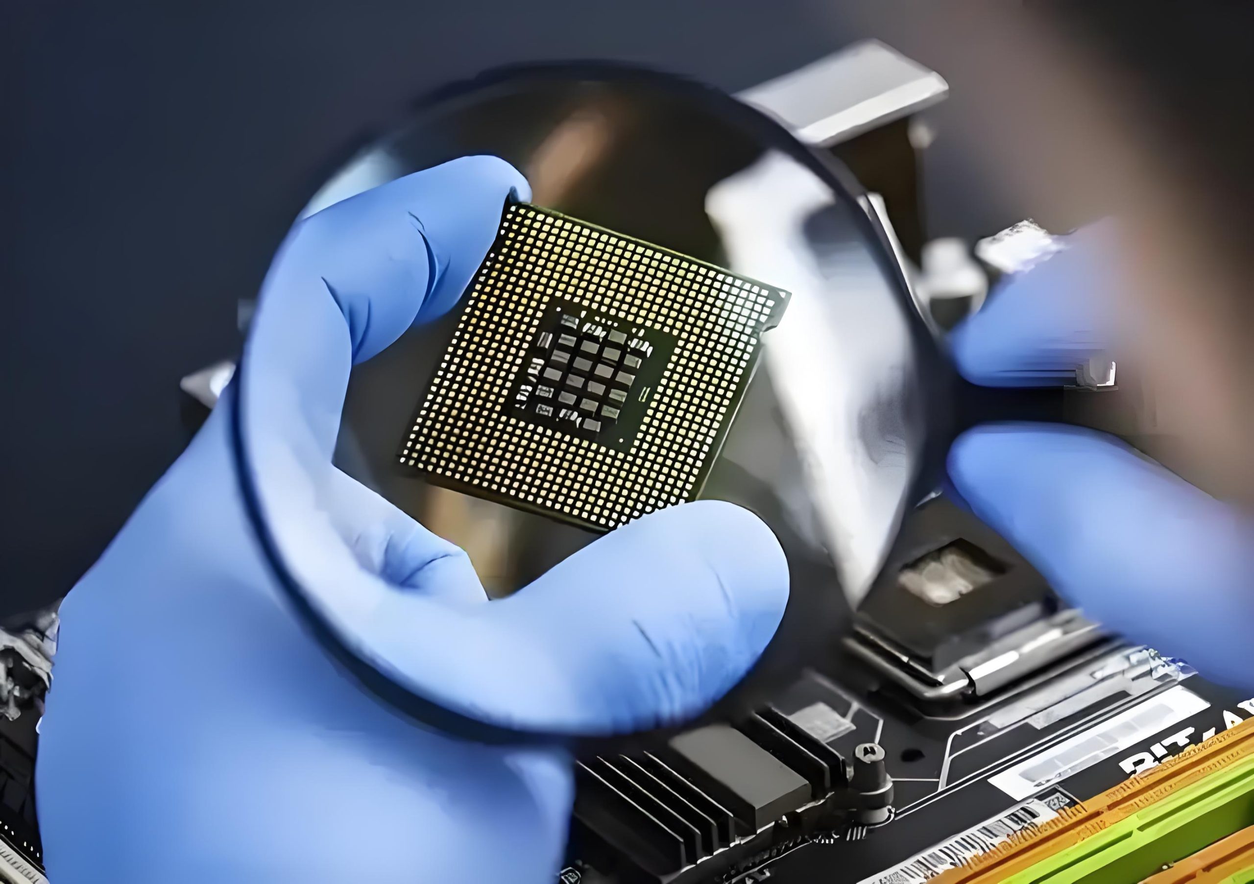
- High reliability packaging structure
Air tightness sealing: glass sealing or metal solder sealing is used, helium leakage rate <1 x 10⁻⁸ ATM·CC³/SEC, meeting MILSTD883 standard
Wide temperature working capacity: 55℃ to +200℃ working temperature range, short term can withstand 260℃ reflow soldering temperature
- Excellent electrical performance
Low parasitic parameters: lead inductance <2NH, supporting high-speed signal transmission above 500MHZ
Stable dielectric properties: dielectric constant 9.4 (1MHZ), loss tangent value <0.001
- Enhanced thermal management capabilities
The thermal conductivity of ALN substrate version is 180W/ (M·K), and the thermal resistance is as low as 15℃/W
Integrated metal heat sink or thermal pad can be used to improve the heat dissipation capacity of power devices
- Compact mechanical design
Typical package thickness 1.02.0MM, saving more than 60% PCB space compared to DIP package
Bending strength> 200MPA, meet the vehicle vibration resistance requirements
- Prominent technical indicators in industrial applications
| qualification | Parameter range | Industry impact
| Number of pins | 832 pins | Suitable for small and medium scale IC packaging
| Pin spacing 0.65MM/0.8MM/1.27MM Compatible with high density SMT assembly process
| Thermal resistance (junction to environment) | 1530℃/W (AL₂O₃ substrate) | Supports stable operation of 15W power devices
| Air tightness grade MILSTD883 METHOD 1014 Ensure a service life of more than 10 years (space/medical)
| High frequency characteristics | Transmission delay <50PS | Suitable for high speed digital circuit design
Compared to plastic SOP (PSOP):
The operating temperature range is expanded by 60% (55℃~+200℃ VS 40℃~+125℃)
The life span is 510 times longer in hot and humid environment
Thermal resistance is reduced by about 40%
- Typical application scenarios
- Consumer electronics and communications equipment
Smartphone RF front end: Compact packaging requirements for 5G millimeter wave bands (28/39 GHZ).
Optical module transceiver: high frequency signal transmission and low loss characteristics are suitable for high speed optical communication (100G PAM4).
- Automotive electronics
ADAS control unit: Camera/radar signal processing chip, resistant to vehicle temperature shock (40°C to +125°C).
Vehicle information and entertainment system: high-density integration to meet the miniaturization requirements of central control screen driver IC.
- Industrial and medical equipment
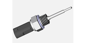
Industrial sensor module: corrosion resistant ceramic is suitable for chemical, oil and gas exploitation and other harsh environment, high temperature pressure sensor.
Portable medical devices: ultra-thin packaging for low-power chips such as blood glucose meters and electrocardiogram monitors.
- Material innovation and performance upgrade
Aluminum nitride ceramics are popularized: the thermal conductivity is increased to 170 W/MK, and the thermal resistance is reduced to less than 10°C/W, suitable for high power density chips (GAN devices).
Composite structure design: ceramic metal composite substrate combines the advantages of both sides to improve mechanical strength and heat dissipation efficiency.
- Integration and multifunctionality
3D stacking technology: multi-layer ceramic substrate vertical interconnection is realized through TSV (silicon through-hole), passive components are integrated (LTCC technology), and peripheral circuit volume is reduced.
Heterogeneous packaging (SIP): integrated with optoelectronic devices and MEMS sensors, and expanded to optical communication modules and intelligent sensing fields.
- Intelligence and green manufacturing
AI-driven process optimization: Machine learning optimizes sintering parameters and thermal field distribution to improve yield and reduce energy consumption.
Application of environmental protection materials: lead-free welding and recyclable ceramic materials are developed to meet ROHS/REACH standards.
- Expansion of emerging areas
Internet of Things (IOT) devices: ultra-low power chip packaging for smart home and wearable devices.
Microsatellite (CUBESAT): lightweight, radiation-resistant ceramics to meet the electronic needs of low-cost satellites
Ceramic SOP packaging has established an irreplaceable position in high-end fields such as aerospace and medical electronics due to its airtightness, wide temperature operating range, and excellent electrical and thermal performance. Driven by technological advancement and market demand, ceramic SOP packaging will transition from “high-reliability specialization” to a new phase of “high-performance popularization.” Over the next five years, ceramic SOP packaging is expected to exhibit the following development trends:
- Performance improvement: high frequency (> 30GHZ) and high thermal conductivity (> 200W/M·K) versions have been introduced
- Cost reduction: Large-scale production makes the price gradually close to high-end plastic packaging
- Application expansion: The penetration rate in emerging markets such as commercial space and smart healthcare will increase to more than 25%


