Core advantages of CQFP
- High density and high performance combined
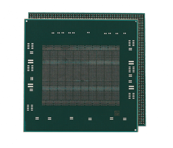
Four-sided lead layout: The leads are distributed on the four sides of the package, supporting high number of leads (usually 64-304 leads), and the spacing can be as low as 0.4MM, which meets the high density integration requirements of complex integrated circuits.
Flattened design: low package height (1.0-4.0MM), compatible with surface mount technology (SMT), suitable for modern high-density PCB layout.
- Excellent reliability and environmental adaptability
Extreme temperature resistance: Ceramic substrate (alumina or aluminum nitride) can withstand-55°C to +175°C, gas tight leakage rate <5 x 10⁻⁸ ATM·CC³/SEC (in line with MIL-STD-883), suitable for high temperature, high humidity and vacuum environment.
Anti-mechanical stress: The ceramic structure has excellent anti-vibration and anti-bending performance, suitable for high vibration scenarios such as vehicle and aerospace.
- High frequency and heat dissipation performance optimization
Low parasitic parameters: short pins and symmetrical layout reduce inductor/capacitor effects, support high frequency signal transmission (10 GBPS), insertion loss <0.5 DB @10 GHZ.
High efficiency heat dissipation: the high thermal conductivity of ceramic substrate (aluminum nitride thermal conductivity 170 W/MK) combined with metal heat dissipation layer, the thermal resistance (ΘJA) is as low as 15-30°C/W, suitable for high power chips.
- Key technical indicators in industrial applications
- Packaging specifications and electrical performance
Pin number and spacing: standard pin number 64-304, spacing 0.4-1.0MM (ultra fine spacing can reach 0.3MM).
Signal integrity: supports high-speed signal transmission (PCIE 4.0), transmission rate> = 16 GT/S, return loss <-20 DB.
- Limit working parameters
Temperature range: military grade-55°C to +175°C, industrial grade-40°C to +125°C.
Thermal cycle capability: through 500 cycles from-65°C to +150°C, the weld point is not cracked.
- Material and process standards
Ceramic substrate process: high temperature co-fired ceramic (HTCC) ensures the density and mechanical strength of multi-layer wiring, alumina purity>96%.
Air tightness verification: helium mass spectrometry leak detection and HAST (high pressure accelerated aging test) to ensure long-term sealing.
- Typical application scenarios
- High frequency communication and computing equipment
5G base station RF module: supports millimeter wave band (28/39 GHZ) signal processing, suitable for high frequency low loss requirements.
Data center switching chip: high pin density to meet the high speed SERDES interface requirements of 100G/400G optical modules.
- Aerospace and defense industry
Satellite navigation processor: radiation resistant ceramics (total dose> 100 KRAD) to ensure long-term operation in space environment.
Airborne radar signal processing: withstand high altitude low temperature (-55°C) and instantaneous power shock.
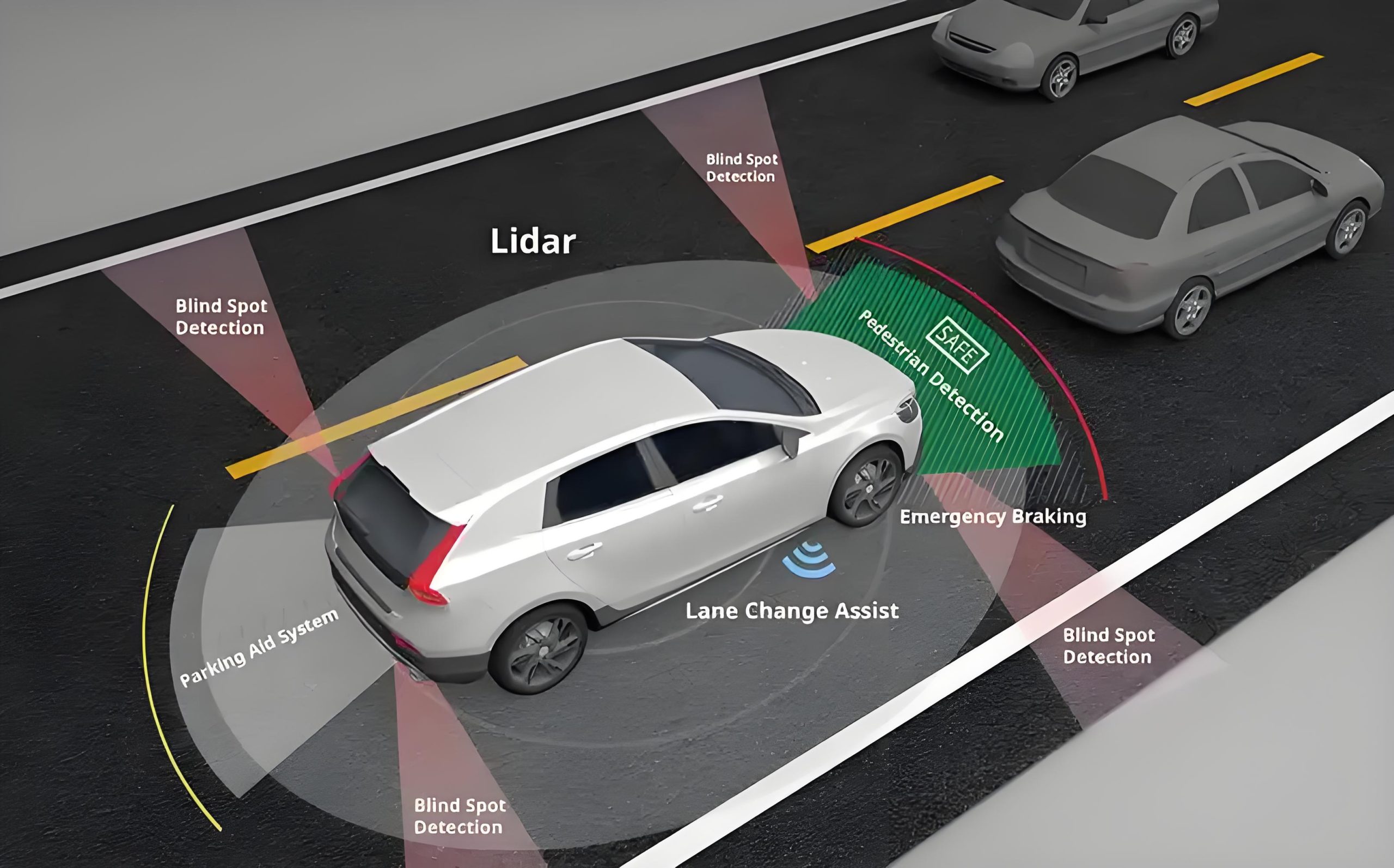
- Automotive and industrial electronics
Autonomous driving domain controller: high density packaging requirements for multi-sensor data fusion chips.
Industrial PLC main control chip: corrosion resistant ceramic is suitable for high temperature and dust environment in chemical plants.
- Ultra-high density and heterogeneous integration
3D-IC stacking: multi-layer interconnection is achieved through silicon through-hole (TSV) and micro-bump technology, and the number of pins exceeds 500+.
Photoelectric co-packaging: integrated laser and silicon photonic chip for CPO (co-packaged optical) module to reduce optical interconnect power consumption.
- Material and process innovation
Aluminum nitride ceramics are popularized: replacing alumina, the thermal conductivity is increased to 170 W/MK, and the thermal resistance is reduced to less than 10°C/W.
Low temperature co-fired ceramic (LTCC): integrated embedded passive components (resistance/capacitance), reducing package volume by 30%.
- Intelligence and green manufacturing
AI-driven design optimization: Machine learning automatically optimizes pin layout and heat dissipation path, increasing yield by 15%.
Lead-free and circular economy: development of bio-based solder and recyclable ceramics, reducing carbon emissions by 40% (in line with the EU Green Agreement).
- Expansion of emerging areas
Quantum computing control module: suitable for ultra-low temperature packaging of superconducting qubits (below 4K), low temperature thermal matching material is the key.
Brain-computer interface chip: miniaturized CQFP (size <5MM²) for implantable neural signal processing.
According to YOLE data, the global ceramic QFP market size is about $1.2B in 2023, and it is expected that:
$1.6B by 2025 (CAGR 10.2%)
Breakthrough $2.5B (CAGR 12.5%) by 2030
Growth drivers:
- Global 5G base station construction (up 25% annually)
- Commercial space development (satellite manufacturing costs reduced by 60 per cent)
- Automotive electronics upgrade (L4 autonomous driving penetration increase)
Ceramic QFP (CQFP) holds a central position in 5G communications, aerospace, and autonomous driving due to its high density, high frequency performance, and military-grade reliability. In the future, with breakthroughs in 3D integration, optoelectronic fusion, and green manufacturing technologies, CQFP will evolve towards ultra-high frequency (Terahertz), ultra-thin (thickness <1 MM), and multifunctional applications, penetrating into cutting-edge fields such as quantum computing and bioelectronics, becoming the cornerstone packaging solution for next-generation high-value-added electronic systems. Its technological iteration path will focus on “higher density, lower power consumption, and broader adaptability,” continuously pushing the boundaries of advanced electronic packaging technology.


