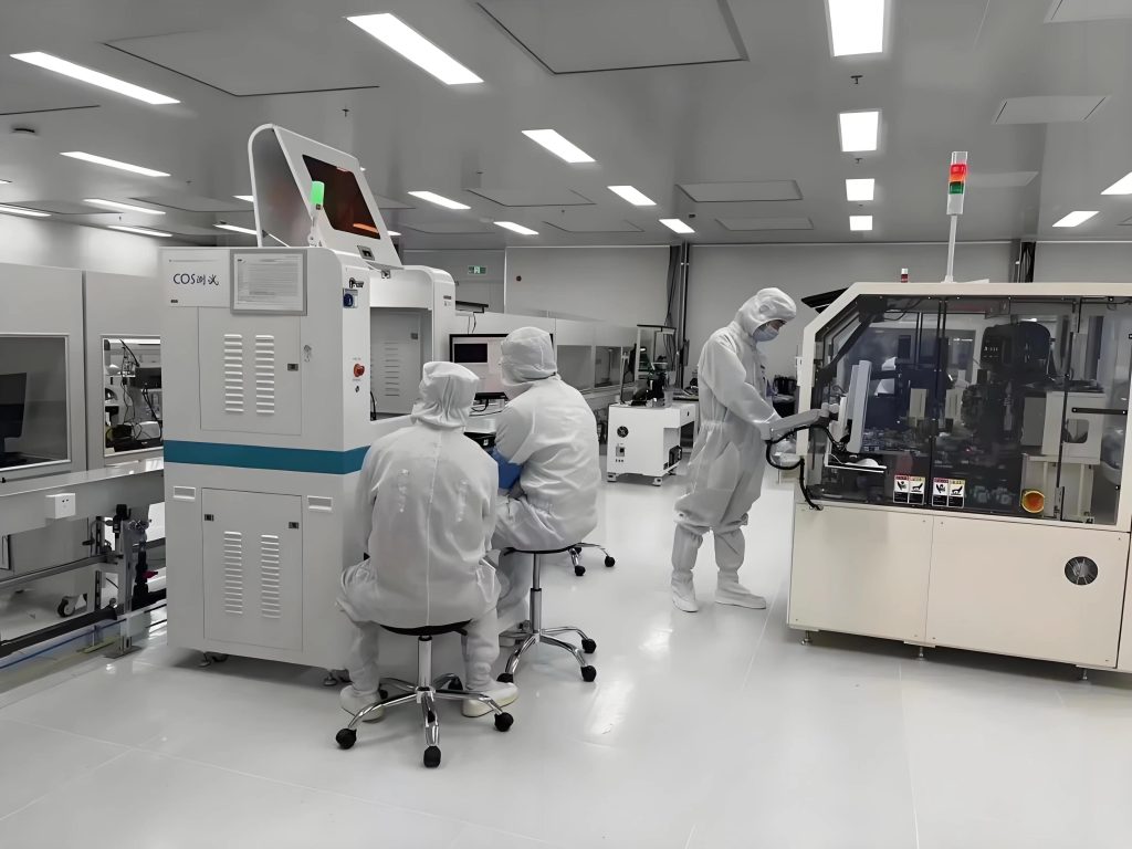
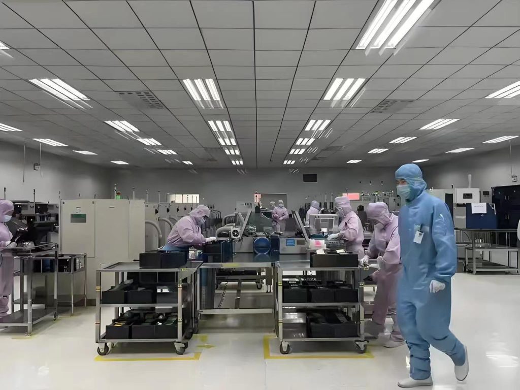
- Improved Siemens process (closed-loop trichlorosilane reduction process)
- Raw material purification: Metallurgical grade silicon (purity> 99.5%) reacts with hydrogen chloride (HCL) to produce trichlorosilicon (SIHCL₃), which is purified by distillation to electronic grade (purity> 99.999999999%,11N).
- Reduction deposition: In the reduction furnace, trichlorosilicon and hydrogen gas undergo chemical vapor deposition (CVD) at high temperature (1100℃~1200℃), and generate high purity polysilicon rod.
- Tail gas recovery: unreacted SIHCL₃ and HCL are recovered through a closed-loop system, and the utilization rate of raw materials is>99%.
- Post-treatment: the polysilicon rod is broken, cleaned and dried to make granular silicon or silicon ingot.
- Fluidized bed method (FBR method)
- Process characteristics: in the fluidized bed reactor, silane (SIH₄) gas is decomposed and deposited through the silicon particle bed to continuously produce granular silicon.
Technical advantages: energy consumption is 30-40% lower than Siemens method, high degree of automation, suitable for large-scale production.
- Metallurgical method (physical purification)
Process: Remove impurities in industrial silicon by physical means such as wet acid washing, oxidation slag making and vacuum smelting.
Advantages: low cost, environmental protection, suitable for solar grade silicon (purity> = 6N).
- Core technology advantages
- Material performance advantages
Purity and impurity control:
◦ The purity of electronic grade polysilicon is greater than or equal to 99.999999999% (11N), and the impurity content is less than 0.1PPB, which supports the manufacturing of advanced semiconductor devices.
◦ The purity of solar grade polysilicon is more than 99.9999% (6N), and the impurity content is less than 1PPM, suitable for high efficiency photovoltaic cells.
Mechanical and chemical stability:
◦ Bending strength>7.0GPA, high temperature resistant (>1410℃), chemical properties stable, acid and alkali corrosion resistant.
Electrical properties:
◦ The resistivity range is 0.001Ω·CM~1000Ω·CM, and the conductivity type and conductivity can be controlled by doping (B, P).
- Apply technical advantages
◦ Conversion efficiency 15%-22% (PERC technology), cost is 30%-50% lower than monocrystalline silicon.
◦ Adapt to distributed power stations and centralized photovoltaic power stations, reducing the cost per kilowatt hour by 20%.
Semiconductor devices:
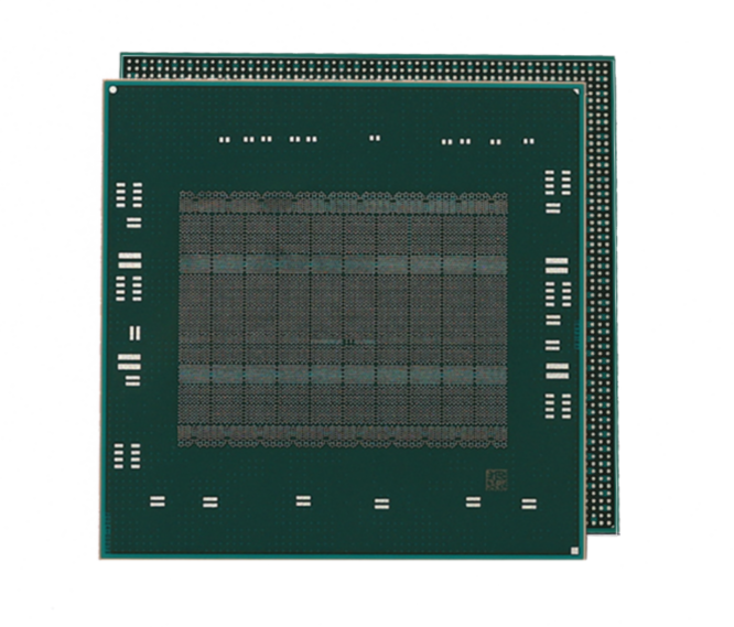
◦ Supports more than 90% of the global semiconductor demand, used in integrated circuits, transistors, sensors and other basic devices.
◦ Adapt to advanced processes below 7NM, and make breakthroughs in the localization of 12-inch wafers.
- New energy and industrial extension:
◦ It is widely used in optical communication, aerospace and other fields, such as satellite communication devices and optical lenses.
◦ Used for motor controllers and charging piles of new energy vehicles, the voltage rating is increased to 1200V.
Key application fields and technical indicators
| Application field | Technical indicators | Advantage comparison (VS monocrystalline silicon)
| Photovoltaic cells | Conversion efficiency of 15%-22% (PERC), cost 30%-50% lower than monocrystalline silicon | Suitable for large-scale power station construction, electricity cost reduced by 20%
| Semiconductor devices | Purity of 99.999999999% (11N) and suitable for advanced processes below 7NM | Supporting more than 90% of global semiconductor demand
| Optical communication device | Transmittance>90%, response speed 100GBPS | Transmission distance increased by 30%, power consumption reduced by 25%
| New energy vehicles | Pressure resistance grade 1200V, high temperature stability>175℃ | Adapt to motor controller and charging pile, improve system efficiency
- Green manufacturing: the Siemens closed-loop circulation system is improved to reduce waste emissions, and the carbon footprint of fluidized bed method is reduced by 80%.
- Large size wafers: technological breakthroughs in 12-inch and above wafers to meet the needs of large-scale production adapted to advanced processes (such as 3NM and below).
- Nano-material composite technology: combined with graphene, quantum dots and so on to improve the efficiency of photoelectric conversion (efficiency can reach more than 23%).
- Flexible applications: Develop ultra-thin flexible polysilicon cells (bending radius <5MM) and expand to wearable devices, drones and other fields.
Polysilicon’s mature manufacturing processes, high cost-effectiveness, and broad applicability dominate the photovoltaic and semiconductor industries. Its technological advantages (such as high purity, low defects, and cost efficiency) will be further expanded through process optimization (like large wafers and flexible silicon wafers) and continuous upgrades in green production technologies. In the future, polysilicon will continue to support global energy transition and industrial upgrading.


