
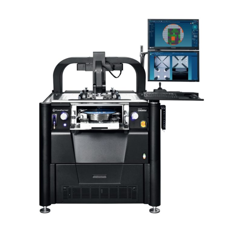
Equipment features: 1. Non-destructive precision testing Micrometer-level probe contact technology (minimum...
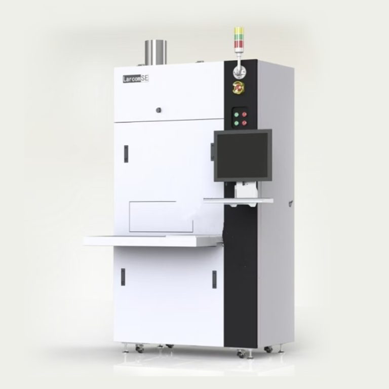
Equipment features: 1. Using maskless direct writing lithography technology, high-precision electron...
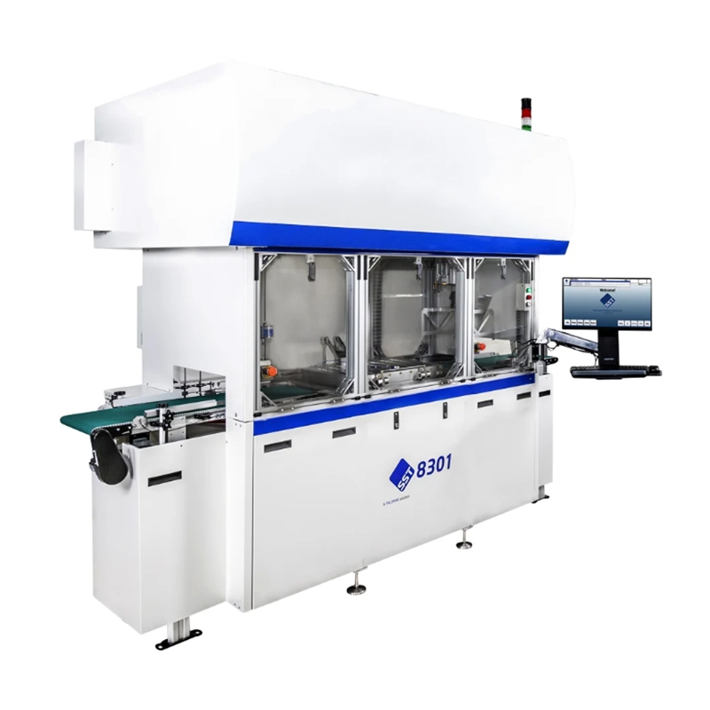
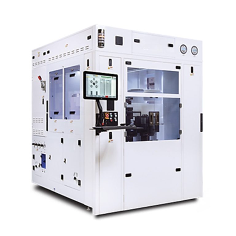
Equipment features: 1. Core advantages Fully automatic high-speed inventory, 20 times more efficient...
Equipment features: 1. Process principle Deposition mechanism: Potential-controlled directional deposition...
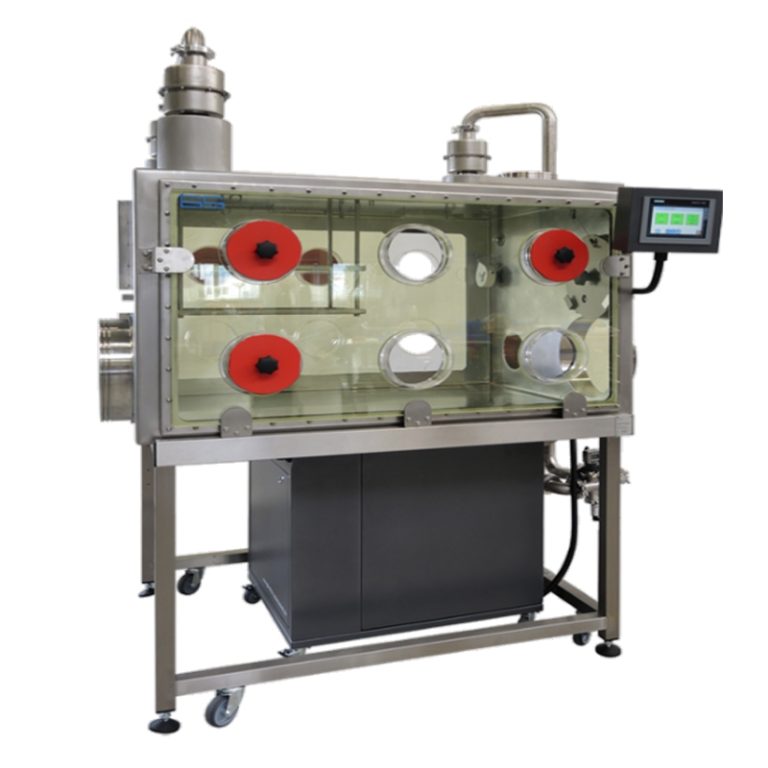
High-purity inert glove box system Equipment features: 1. Ultra-pure environment control O₂/H₂O<0.1ppm...
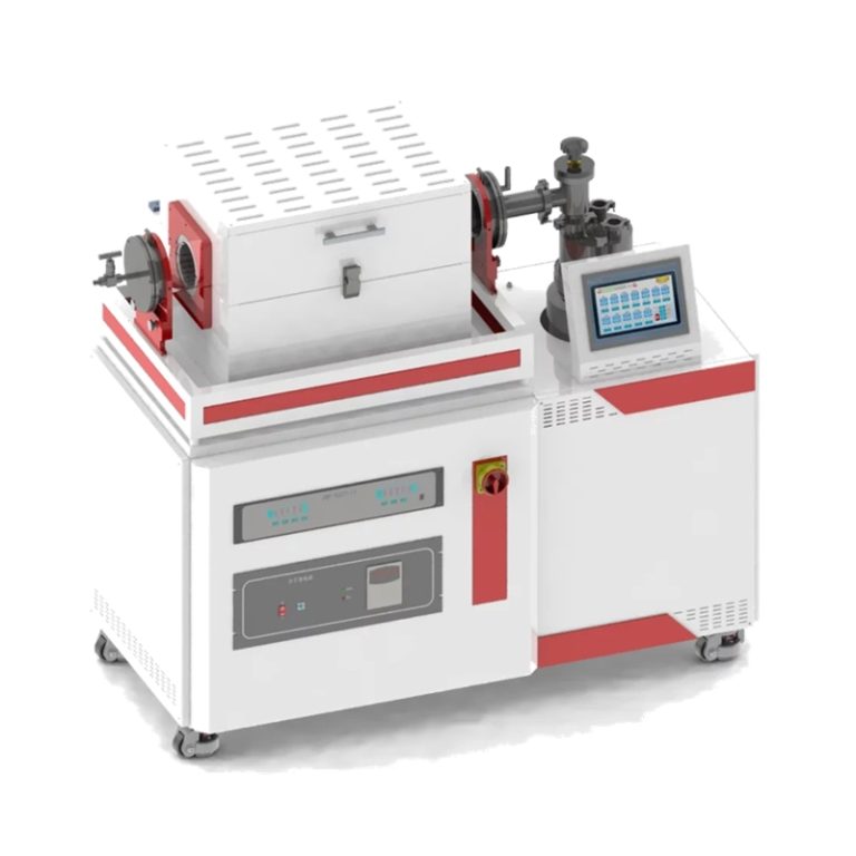
Tunnel furnace 1. Equipment features: Continuous conveyor belt/track conveyor Multiple temperature zones...
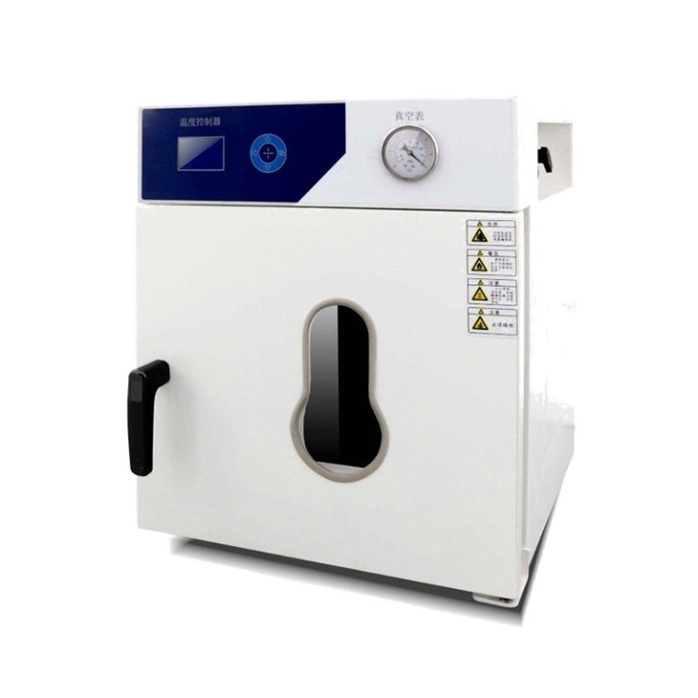
Vacuum furnace 1. Equipment features: Working temperature: 0-250℃ Ultimate vacuum: 133Pa Furnace volume:...
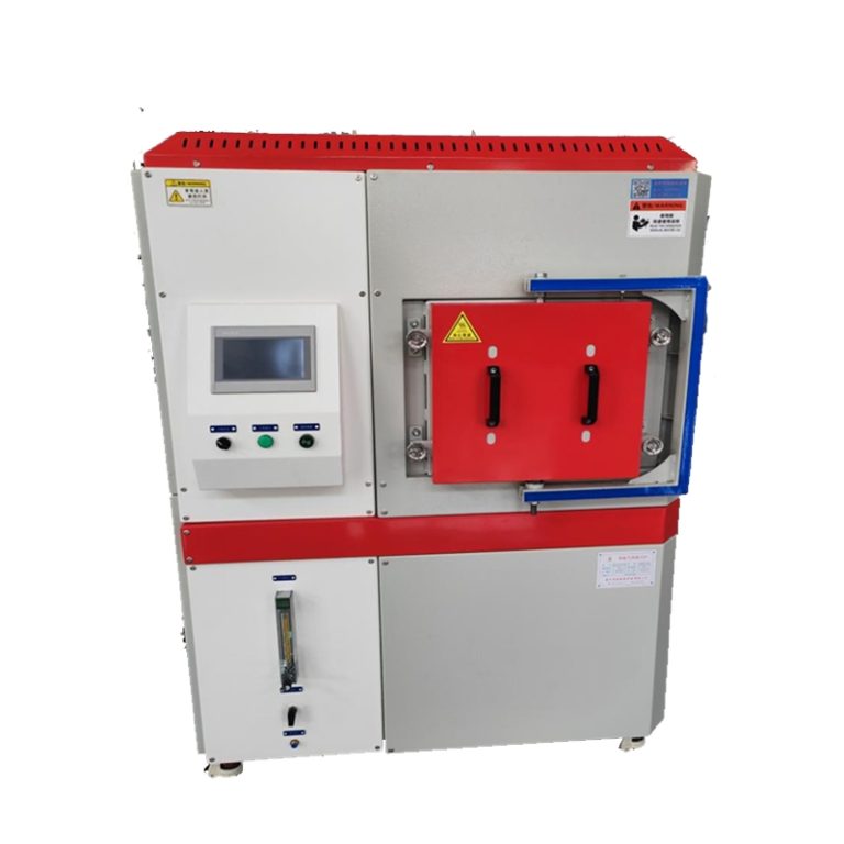
High temperature furnace 1. Core parameters Limit temperature: 1500-1800℃ Working temperature: 1450-1750℃...
1. Core performance Temperature range: 200-1300℃ Temperature change rate: ≤150℃/s (standard bare die...
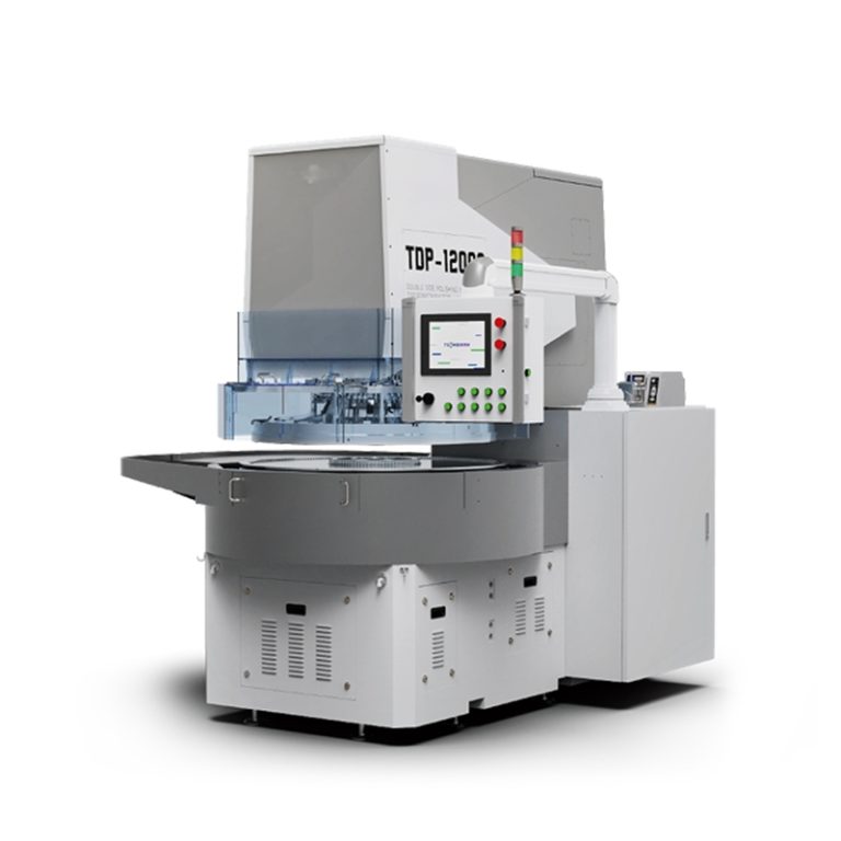
1. Core functions Global surface flattening Single/double-sided polishing process Multi-material compatible...
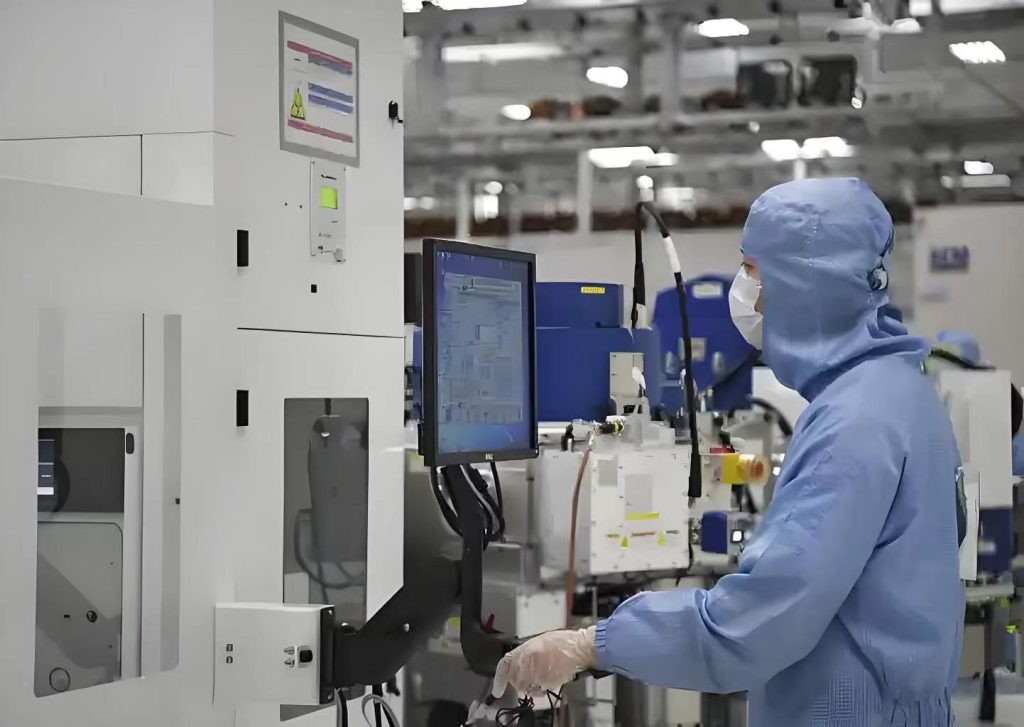
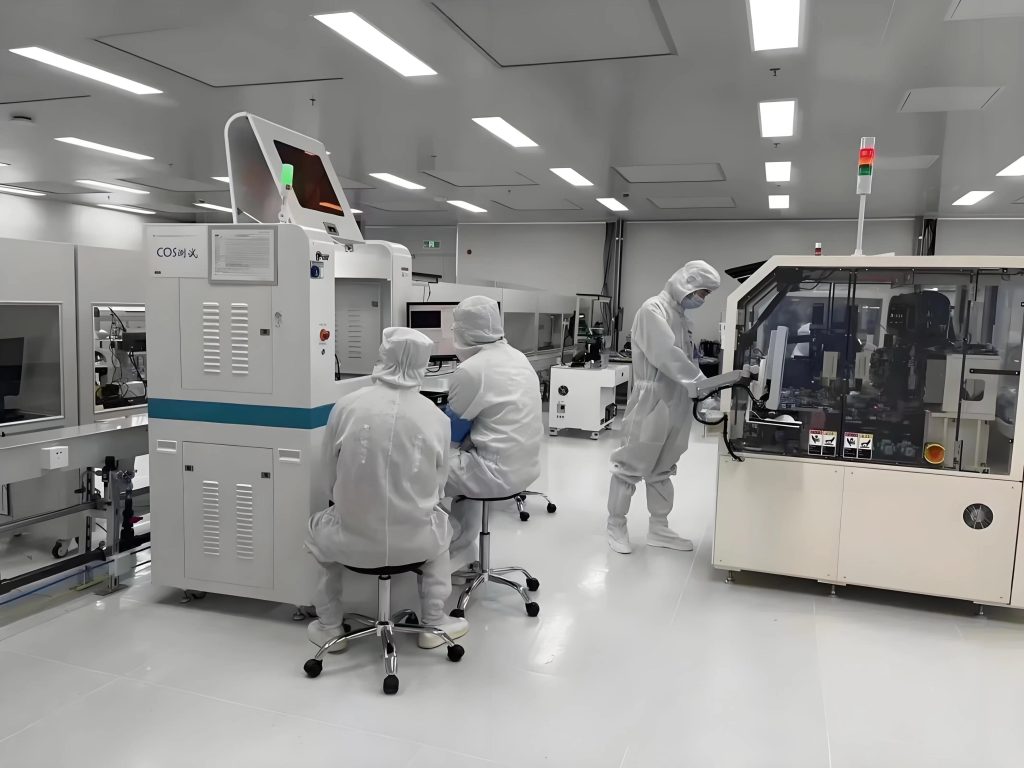
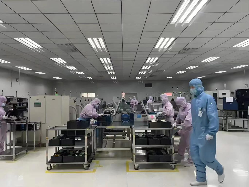
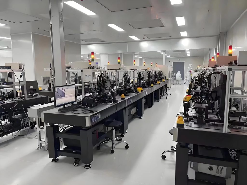
Title: Semiconductor manufacturing processes Objective: To have a certain foundation for the overall...


