- Core process of monocrystalline silicon manufacturing
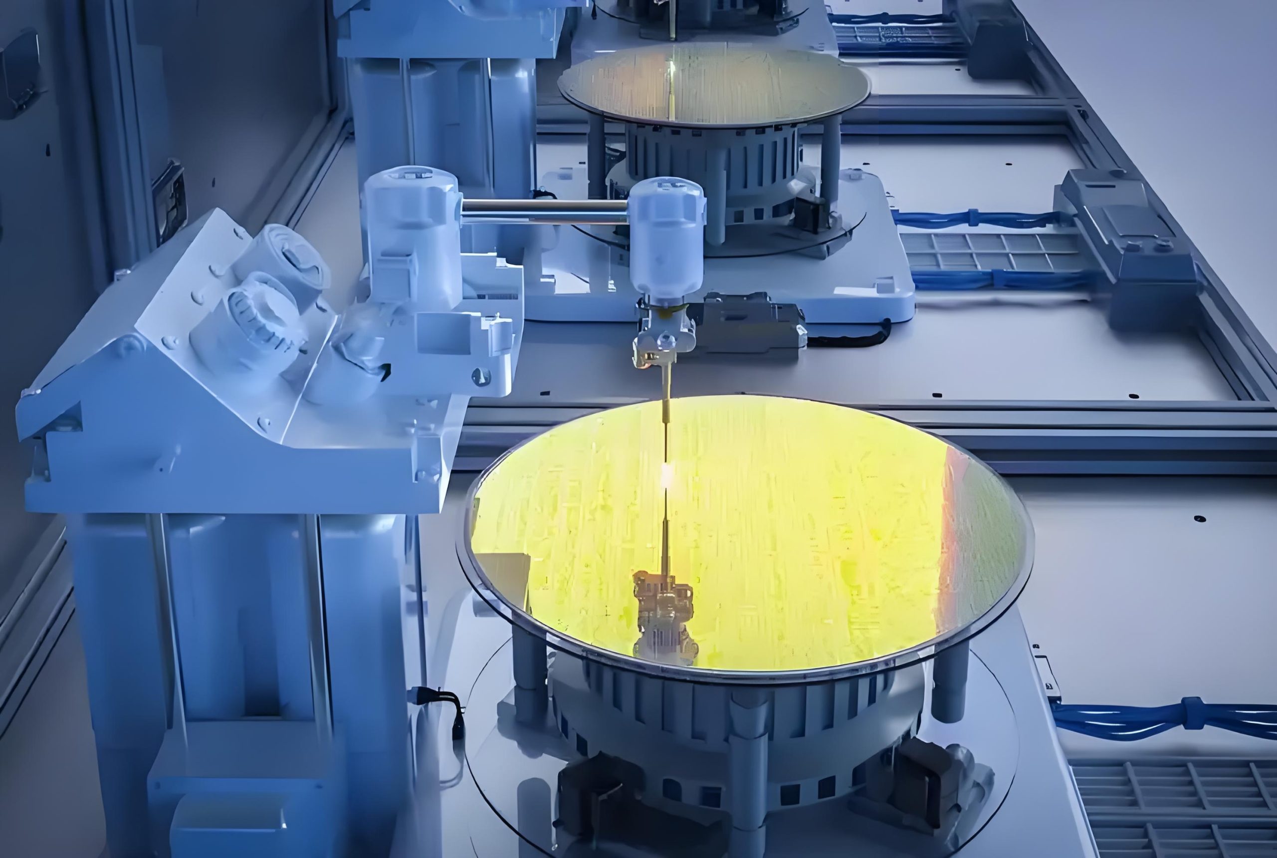
- Direct pull (CZ method)
Raw material preparation: use electronic grade polysilicon (purity> 99.9999%), crush into uniform particles and put into quartz crucible, melt in high temperature (above 1414℃) in inert gas (argon) environment.
Crystal growth:
- Intriging: The single crystal seed crystal is immersed in the molten silicon liquid, and the single crystal silicon rod is gradually formed by accurately controlling the temperature gradient (±1℃), seed crystal rotation speed (6-12 rpm) and pulling speed (1-6MM/min).
- Segmented control of crystal rod: adjust parameters (speed, gas flow rate, lift rate) in three stages. In the first stage, inert gas flow rate is 60-80L/MIN, and in the third stage, it is increased to 150-200L/MIN, so as to reduce axial temperature gradient and reduce the risk of crystal cracking.
- Cooling and post-treatment: The crystal rod is annealed to eliminate thermal stress, cut into silicon ingot, and then polished by outer diameter grinding, slicing (diamond wire or inner circle cutting), chamfering (reducing edge stress), chemical corrosion (removing surface damage layer), and CMP polishing (surface roughness <1NM).
2.Zone melting method (FZ method)
- For high power semiconductor devices, no crucible is required, polycrystalline silicon rod is locally melted by high frequency coil, combined with seed crystal oriented crystallization, the impurity content is lower (purity can reach 99.9999999%).
Advantages: Avoid quartz crucible contamination, suitable for manufacturing high resistivity (>1000Ω·CM) monocrystalline silicon, but the cost is higher and the diameter is limited to less than 200MM.
- Core technology advantages
- Material performance advantages
- High purity and low defect: the impurity content of Czochralski monocrystalline silicon is less than 0.1PPB, and the lattice defect density is less than 0.1/CM², which ensures the yield of chips (the yield rate of TSMC 3NM process is 92%).
- Bandable structure: 1.12EV bandgap balanced switch characteristics (off-state leakage current as low as 1NA/ΜM) and power consumption are better than wide bandgap materials such as gallium nitride.
- Mechanical stability: bending strength 7.0GPA, Young’s modulus 190GPA, fragmentation rate <0.01% (GAAS substrate fragmentation rate>5%), suitable for hundreds of chip manufacturing processes.
- Ultra-high purity and low defect density
- Purity grade (>= 99.9999%), the impurity content of 12N grade monocrystalline silicon is less than 0.1PPB, and the leakage current is reduced by 60%.
- Low defect density (<0.1/CM²), improve the yield of chips to more than 92%, and avoid production loss caused by material defects.
3 Excellent thermal stability and mechanical strength
- High temperature performance: can withstand working temperature above 175℃, suitable for extreme environment of automotive electronics and aerospace devices.
- Mechanical strength: bending strength of 7.0GPA and Young’s modulus (measuring material stiffness) of 190GPA, ensuring that the chip breakage rate is less than 0.01% in hundreds of manufacturing processes, reducing the cost of scrap caused by process damage.
- Process compatibility advantage
- Natural oxidation layer: 1-1.5NM SIO₂ passivation layer is spontaneously formed on the surface to reduce the interface state density (<1E10/CM·EV) and simplify the manufacturing process of MOSFET devices.
- Bipolar doping capability: N-type electron mobility 1500CM²/V·S, P-type hole mobility 450CM²/V·S, supporting CMOS process (99% of the world’s transistors depend on this feature).
- Metal compatibility: ohmic contact with titanium/cobalt (resistance as low as 1E-7Ω·CM), thermal expansion coefficient matching tungsten plug, ensuring the reliability of interconnection structure.
- Band structure and electrical properties
- 1.12EV intrinsic band gap balanced switch characteristics and power consumption, the off-state leakage current is as low as 1NA/ΜM, better than gallium nitride and other materials.
- Bipolar doping capability: N-type electron mobility 1500CM²/V·S, P-type hole mobility 450CM²/V·S, meet the requirements of CMOS process, avoid design compromise due to material limitations.
6 Cost-effectiveness and long-term returns
- Compared with polysilicon: “The power generation of monocrystalline silicon components in the whole life cycle is increased by 20%”, and the investment recovery period of photovoltaic power stations is shortened by 3 years.
- Manufacturing economy: Thousands of chips can be cut from a single 12-inch wafer, and large-scale production reduces customer procurement costs.
- Natural oxidation layer (1-1.5NM SIO₂) eliminates the need for additional passivation process and reduces equipment investment costs.
Supports heterogeneous integration (silicon-based gallium nitride RF devices) and strain engineering (electron mobility increased by 2 times) to reserve space for technology upgrades.
- Application advantages
- Photovoltaic field: conversion efficiency of 24% (polysilicon only 18-20%), combined with PERC cell technology, the cost per KWH is reduced by 30%.
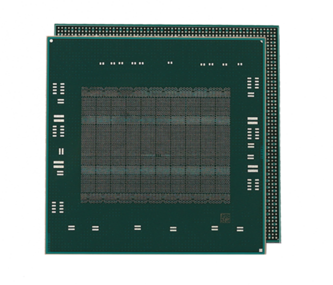
- Semiconductor manufacturing: Supporting advanced processes below 7NM, 12-inch wafers can cut thousands of chips at a time, with significant cost advantages at scale.
- Aerospace: excellent radiation resistance, used in satellite communication RF devices (the axial temperature gradient control technology of crystal rod improves the yield by 20%).
Monocrystalline silicon, with its high purity, low defects, and excellent electrical properties, holds the technological high ground in photovoltaics, semiconductors, automotive electronics, and other fields. Through process optimization using Czochralski and zone-refined methods, its technical specifications (conversion efficiency, voltage rating, yield) continue to improve. Coupled with the cost advantages of large-scale production, it is expected to become a core material for high-performance electronic devices in the future


