- The manufacturing process of graphene
1. Mechanical stripping method (SCOTCH TAPE method)
Process: High oriented pyrolytic graphite (HOPG) is repeatedly peeled off with tape until a single layer of graphene is obtained.
characteristic: The highest purity (defect rate <0.1%) but very low yield (micron-sized fragments). Suitable for laboratory basic research (such as verification of quantum Hall effect).
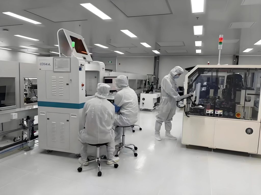
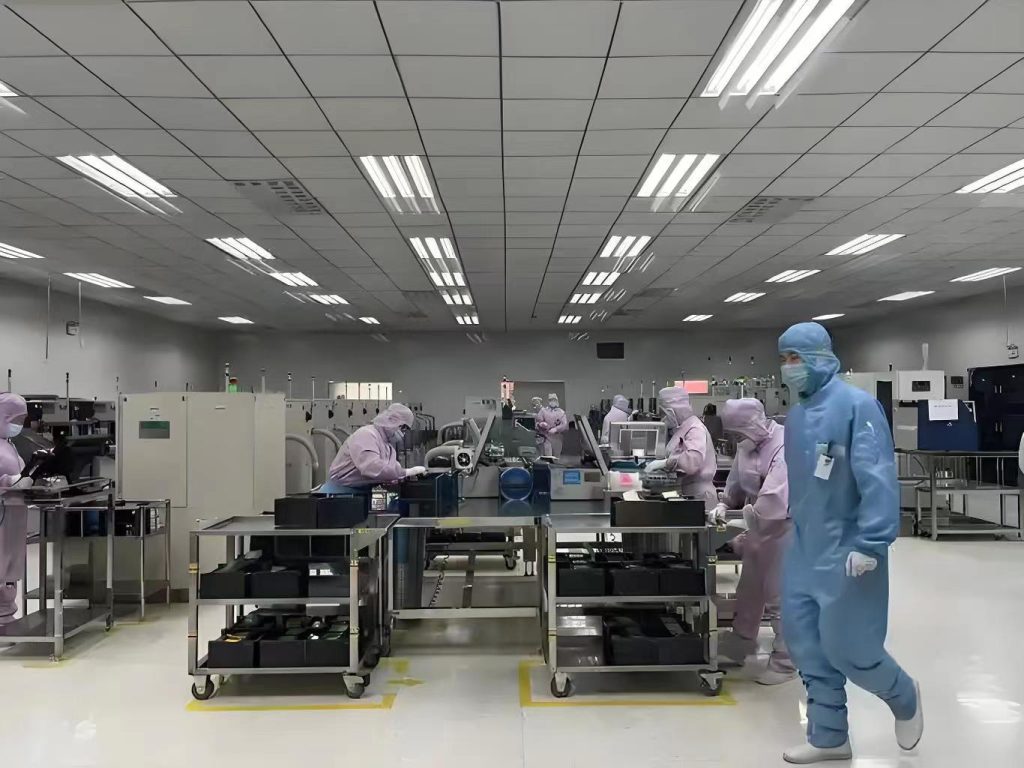
2. Chemical vapor deposition (CVD)
flow path:
1. The metal substrate (copper/nickel) is annealed at high temperature (1000℃) to form a flat surface;
2. Methane (CH₄) and other carbon sources are introduced to catalyze the cracking of carbon atoms;
3. Carbon atoms self-assemble into graphene films;
4. Transfer to the target substrate (such as SIO₂/SI or flexible PET) by etching.
characteristic:
Continuous thin films can be prepared at wafer level (more than 30 inches);
Industrial-grade core processes, such as Samsung and Huawei, are used for flexible screens.
3. REDOX method
flow path:
1. Graphite is strongly oxidized by concentrated sulfuric acid/potassium permanganate to produce graphene oxide (GO);
2. GO ultrasonic dispersion into a single layer solution;
3. Chemical reduction (hydrazine hydrate, ascorbic acid) restores conductivity.
characteristic:
Low cost (<$50/G), suitable for mass production;
4. Liquid phase stripping method
Process: Graphite powder is dispersed in solvent (NMP, DMF), and then peeled into single layer graphene by ultrasonic or high pressure homogenizer.
characteristic:
Yield up to 80% (British HAYDALE technology);
Suitable for printed electronics (ink concentration up to 5 MG/ML).
- Material properties of graphene
1. Physical and chemical properties
| performance index | Values/characteristics |Compare materials (such as silicon, copper) | |carrier mobility | 200,000 cm²/(V·s)(theoretical value) | silicon:1,400 cm²/(V·s)
| heat conductivity | 5,300 W/(m·K)(single layer) | copper:400 W/(m·K)
| tensile strength | 130 GPa | steel:0.4 GPa
| light transmittance | 97.7%(550 nmwavelength) | ITO(Indium Tin Oxide):~90%
| specific area | 2,630 m²/g | acticarbon:1,000-3,000 m²/g
| chemical stability | Able to resist acid and alkali (except strong oxidizing acid) | The metal is easily corroded
2. Unique quantum effect
Quantum Hall effect: at low temperature and strong magnetic field, the conductivity is quantized step (precision up to 10⁻⁹, used for resistance standard). Dirac cone band structure: zero mass fermion properties, supporting ultra-fast electron transport.
- Industry application and technical index advantages
1. Electronics and semiconductor devices
high frequency transistor:
Advantages: carrier mobility is 140 times that of silicon, and the operating frequency exceeds 300 GHZ (IBM 2023 prototype).
Technical indicators: Cut-off frequency (Fₜ) up to 700 GHZ, power density 1.5 W/MM (1.2 times that of GAN).
Flexible electronics:
Application: Foldable screen mobile phone (HuaweiMATE XS uses graphene heat dissipation film).
Advantages: Flexibility> 1 million times (resistance change <2%), transmittance> 97%.
2. Energy storage and conversion
Lithium-ion battery:
Graphene conductive agent: adding 1% graphene, the internal resistance of the battery is reduced by 20%, and the cycle life is increased by 30% (Ningde Times technology).
Silicon-based anode: capacity up to 2,000 MAH/G (traditional graphite anode 372 MAH/G).
Supercapacitors:
Technical indicators: energy density 30 WH/KG, power density 100 KW/KG (MAXWELL TECHNOLOGIES data).
3. Composite materials
aerospace:
Graphene reinforced aluminum matrix composites: 50% strength increase, 20% weight reduction (part of Boeing 787).
Thermal management materials: thermal conductivity increased to 400 W/ (M K) (traditional polymers <1 W/ (M K)).
Lightweight car: graphene/epoxy composite material improves impact resistance by 80% (Tesla battery case).
4. Biomedicine and sensors
biosensor:
Detection limit: 0.1 PG/ML (Novel Coronavirus antigen detection, 1000 times more sensitive than ELISA).
Response time: <5 seconds (glucose sensor).
Antibacterial dressings: The killing rate of Staphylococcus aureus by graphene oxide dressings was>99.9% (3 hours of contact).
5. Environmental engineering
Seawater desalination membrane:
Performance: water flux 200 L/ (M² H BAR), salt retention rate 99.9% (MIT 2022 annual experimental data).
Pollution adsorption: Graphene aerogel adsorbs crude oil at a weight ratio of 86 times (ExxonMobil’s offshore oil spill emergency plan).
- Technical Challenges and Future Directions
1. Scale production: CVD cost needs to be reduced to <$50/M² (currently ~$200/M²).
2. Number of layers control: the proportion of single layer graphene should be>95% (about 80% by CVD method at present).
3. Doping technology: precise control of nitrogen/boron doping concentration (target: carrier density 10¹³ CM⁻²).
4. Heterogeneous integration: interface engineering of graphene with GAN and SIC (interface resistance <1 Ω MM).
Graphene has achieved breakthroughs in semiconductors, new energy, biomedical and other fields with its ultra-high electrical conductivity, mechanical strength, light transmittance and chemical stability:
5G communication: graphene RF devices improve efficiency by 40% in the 28 GHZ band;
Space heat dissipation: the weight of satellite thermal control system is reduced by 30%, and the heat dissipation efficiency is increased by 50%;
Medical diagnosis: Ultra-sensitive sensors drive early cancer detection.
With the maturity of technologies such as roll-to-roll CVD and atomic layer deposition (ALD) doping, graphene is expected to make the leap from “lab miracle” to “industrial pillar material” by 2030.


