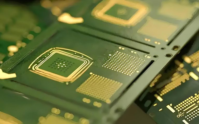
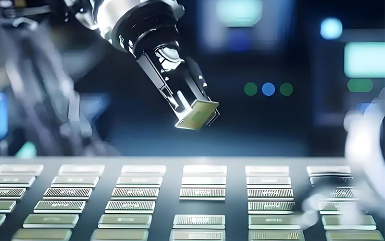
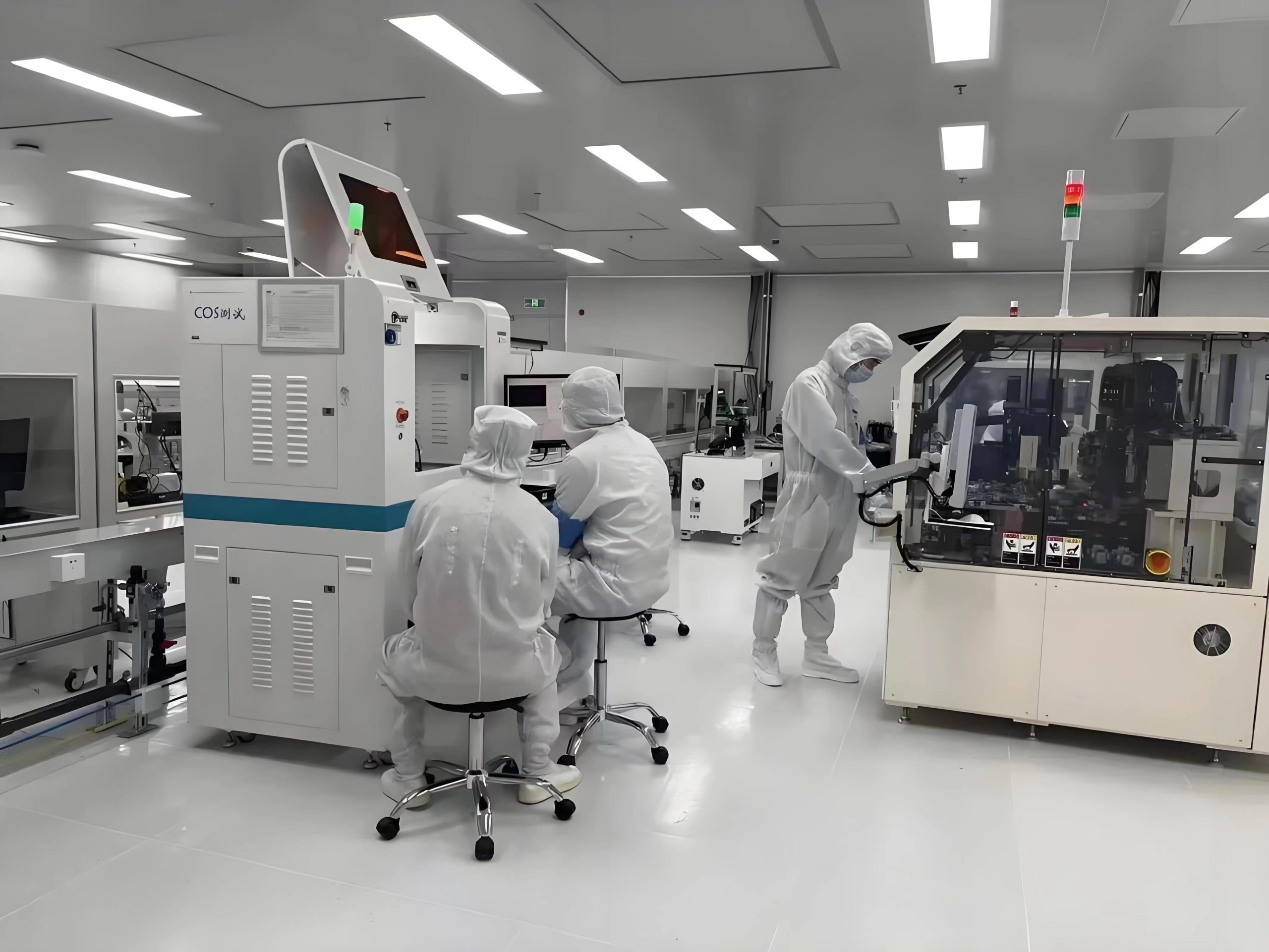
- Preparation of single crystal
Liquid Sealing Direct Drawing Method (LEC Method): In a high-pressure single crystal furnace, boron nitride (PBN) crucibles and dry boron oxide liquid sealants are used to directly synthesize and draw undoped, semi-insulating gallium arsenide single crystals with diameters ranging from 100 to 150 millimeters. The gallium arsenide crystals are then cut into wafers (typically 150-300 ΜM thick), followed by polishing, cleaning, and surface treatment.
- Epitaxial growth technology
Vacuum phase epitaxy (VPE): commonly used GA/ASCL3/H2 system, high purity epitaxial layer growth is achieved by controlling the reaction conditions, suitable for microwave device manufacturing.
Liquid phase epitaxy (LPE): Using GA/GAAS melt cooling growth, gallium and arsenic are dissolved in the molten liquid at high temperature, and gallium arsenide crystals are formed by crystallization through cooling. The growth rate is fast, and large area epitaxial growth can be achieved, which is mainly used for heterojunction structures (such as GAAS/ALXGA1-XAS), supporting laser and solar cells and other devices.
Molecular beam epitaxy (MBE): In ultra-high vacuum environment, the thickness, doping concentration and growth rate of the epitaxial layer are precisely controlled. Gallium and arsenic atoms are deposited layer by layer through molecular beam to form high quality single crystal thin film, and the grown thin film has high quality.
Metal organic compound vapor deposition (MOCVD): Using metal organic compounds (trimethyl gallium) and hydrogen arsenide (ASH₃) to react at high temperature, gallium arsenide thin film is generated, suitable for superlattice structure; fast growth rate, suitable for large area production, can achieve high uniformity and high repeatability of epitaxial growth, widely used in LED and solar cell production.
- High purity requirements
High purity gallium (GA) and arsenic (AS) as the main raw materials need to reach 6N (99.9999%) or 7N (99.99999%) purity, through physical and chemical reactions to synthesize gallium arsenide polycrystal, and then through single crystal growth and cutting processing to make substrates or epitaxial materials.
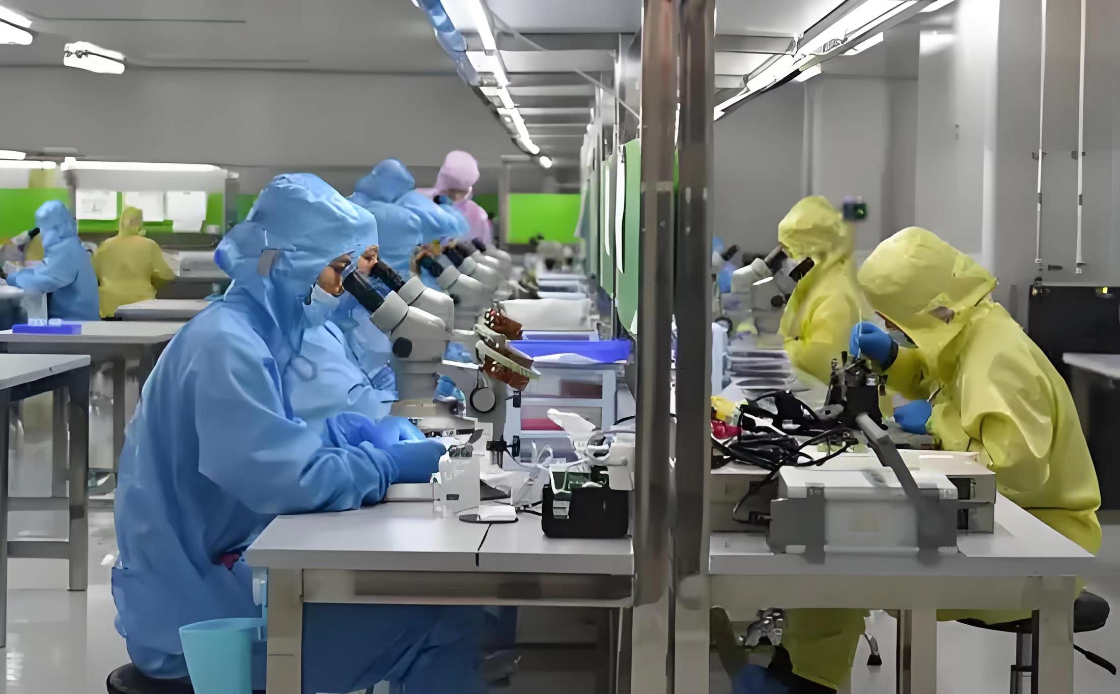
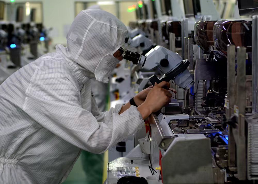
- Core process
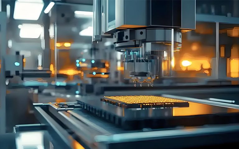
Substrate treatment: The gallium arsenide substrate is annealed (800-850℃) to reduce the resistivity and the active layer is formed by ion implantation.
Lithography and etching: source and drain electrodes are formed by stripping process, device structure is defined by lithography technology, and gate trench shape is optimized by multiple etching.
Passivation and thinning: the device surface is protected by a passivation layer, and the substrate is thinned to improve heat dissipation performance (spacecraft applications).
- Advantages of application technical indicators
- Technical performance
Through ion implantation or diffusion technology, silicon (SI), zinc (ZN) and other elements are incorporated to adjust the electrical properties of gallium arsenide, and transistors, lasers, solar cells and other devices are manufactured using lithography, etching, deposition and other processes,
High electron mobility: The electron mobility is 8500 CM²/ (V·S), which is 5-6 times that of silicon (much higher than silicon’s 1400CM²/V·S). It is suitable for high frequency and high speed components (5G chips, radar). The breakdown electric field strength is 4×10⁵V/CM, which is suitable for high power RF devices.
Direct band gap structure: The direct band gap characteristic makes its light emission wavelength accurate (near infrared 900NM). It is used for remote control and optical communication module. The conduction band and valence band transition does not need phonon assistance, and the light emission efficiency is high, supporting laser, LED and other optoelectronic devices and detectors.
Negative resistance effect: the current decreases with the increase of voltage under high electric field, which is used in microwave oscillation devices.
High-speed digital circuits: Gallium arsenide resistivity (10⁷-10⁹ Ω·CM) significantly reduces microwave transmission for use in ultra-high speed computers and signal processing systems
Photoelectric conversion rate: Gallium arsenide single-junction solar cells can achieve a conversion efficiency of 28%, and multi-junction cells can achieve an efficiency of more than 40% (silicon cells are about 22%), which is widely used in satellites and spacecraft
High frequency and low noise: Field-effect transistors (MESFET) and high electron mobility transistors (HEMT) can operate at frequencies up to 60GHZ with a noise factor of less than 1DB, suitable for low noise amplifiers (LNA).
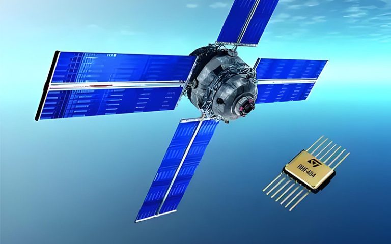
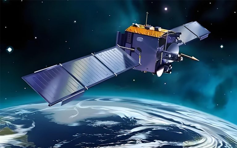
Environmental adaptability: heat resistance and radiation resistance: thermal conductivity is 55W/M·K, higher than silicon’s 150W/M·K, suitable for high temperature working environment, strong resistance to high energy particle irradiation, suitable for aerospace and military environment.
Semiconductor insulation: the substrate is electrically isolated by ion implantation to reduce device interference and improve integration.
- Competitive advantages of gallium arsenide materials
- High frequency communication field
Compared to silicon-based devices, gallium arsenide PA improves efficiency by 20% and power consumption by 30% in 5G base stations.
- Photovoltaic field
Gallium arsenide multi-junction solar cells have an energy density 50% higher than silicon cells for satellite applications.
- Optoelectronics
The modulation bandwidth of gallium arsenide laser can reach 10GHZ, suitable for high-speed optical fiber communication.
- Cost optimization
The cost of gallium arsenide manufacturing is reduced by improving MOCVD process and wafer recovery technology.
- Development of new devices
Develop flexible gallium arsenide solar cells, quantum dot lasers and other new devices.
- Application extension
Promote gallium arsenide devices in autonomous driving, Internet of Things (IOT) and 6G communications.
Gallium arsenide materials, through advanced crystal growth technology and high purity control, show irreplaceable advantages in the fields of high frequency, photoelectricity and radiation resistance, and promote the technological innovation in communication, aerospace, national defense and other industries, occupying a key position in high-end applications.


