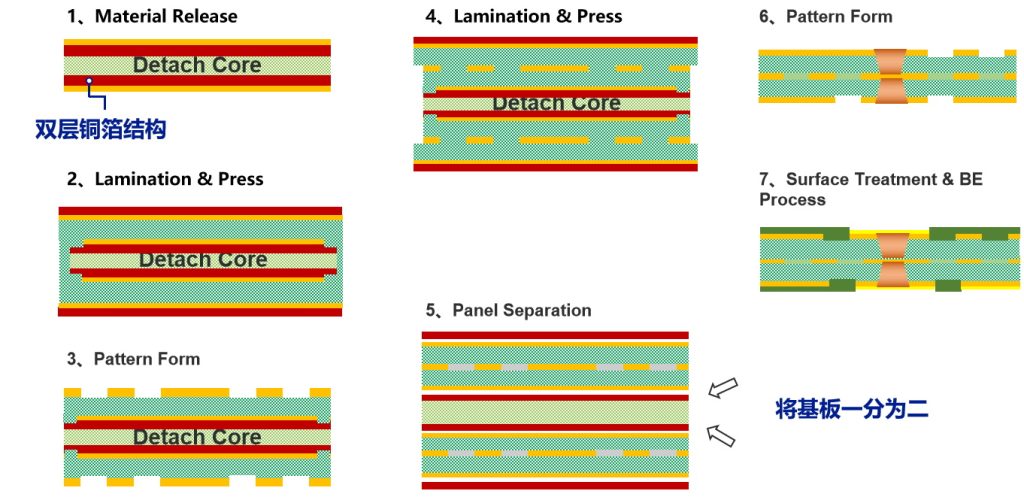
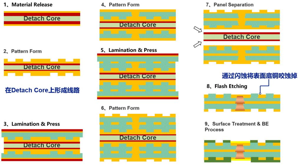
Process schematic diagram
Introduction
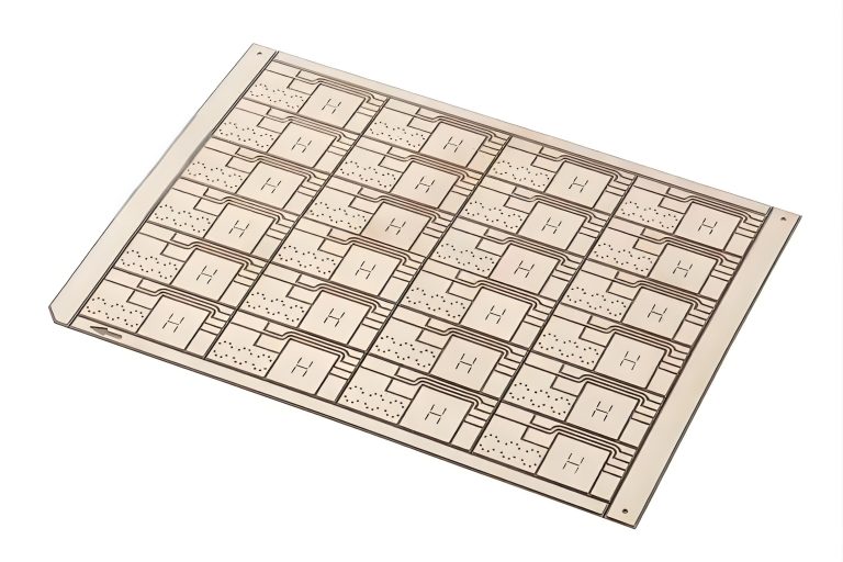
ETS(Embedded Trace Substrate) process, is a kind of coreless process, the difference is: There is a the circuits pattern layer formed on the surface copper foil of detach core, and then laminating prepreg on the circuits pattern layer which the fine trace is embedded in the dielectrics; separating the multi-layer board to two boards; removing the surface copper by etching and forming a “Embedded Trace”Layer finally.
The ETS substrate is used in extremely high intensive I/O count applications, such as memory chips, and the process is as follows
Process schematic diagram

Ceramic thin-filmvacuum sensor Optical gas massflowmeter Liquid mass flowmeter Force sensor MEMS...

Photoelectric sensing chip Light source chips Optical transmission and modulationchips Optical detection...

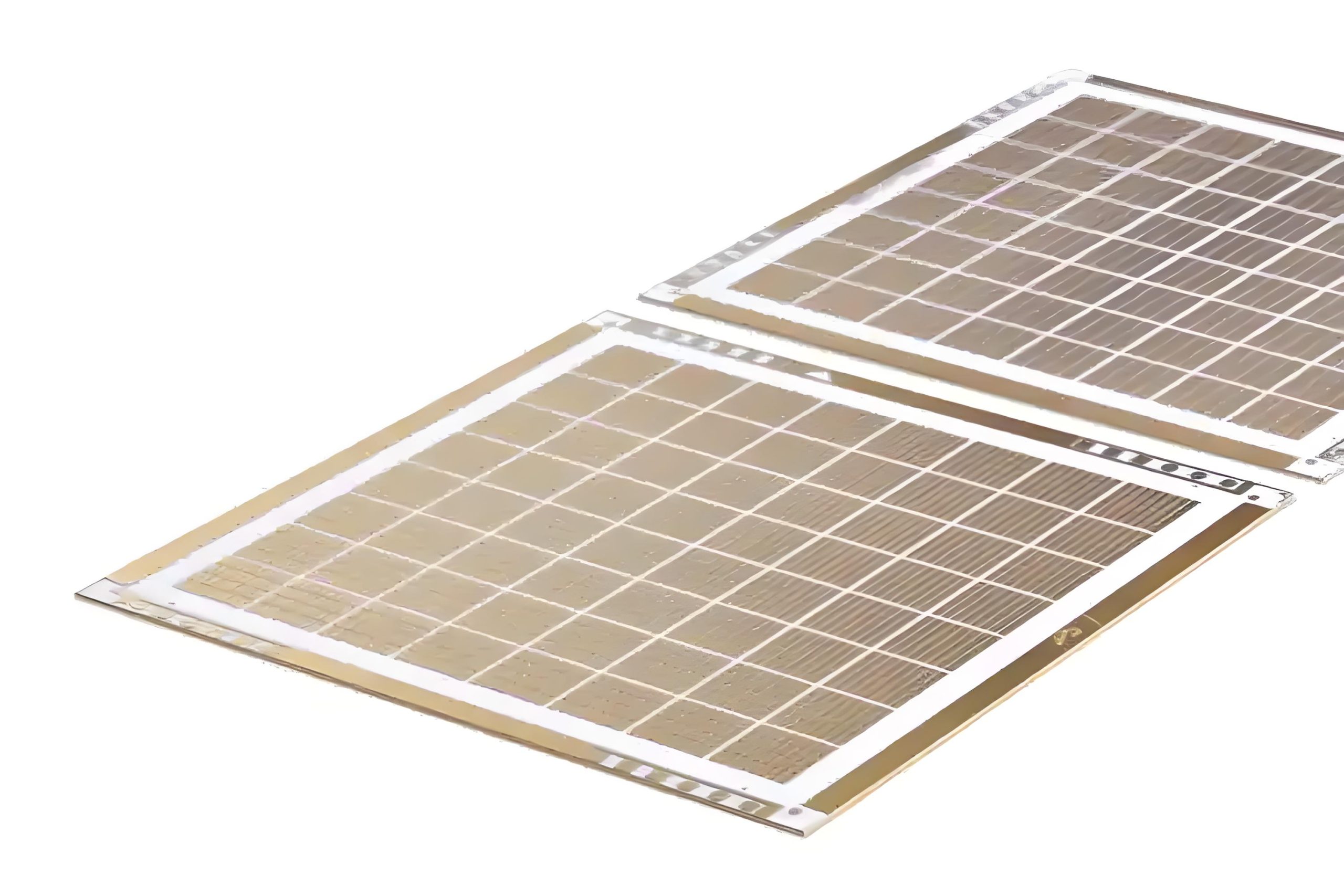
Using a“Detach Core”which has two-layers carrier foil structure on the surface as a core, and forming...
Tenting process is a kind of subtractive process, the process as follows: Laminating photosensitive film...

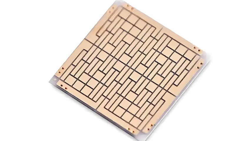
Modified Semi-Added Process abbreviated as mSAP, which can be used on the core or build-up layers, pattern...

Semi-Added Process abbreviated as SAP, using on the build-up-layer pattern forming as follow:First depositing...
The product generally adopts the pressing lamination process of semi-curing sheets , and line formation...
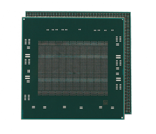
The products generally adopt the Build-up Film Lamination process, and the circuit formation uses the...
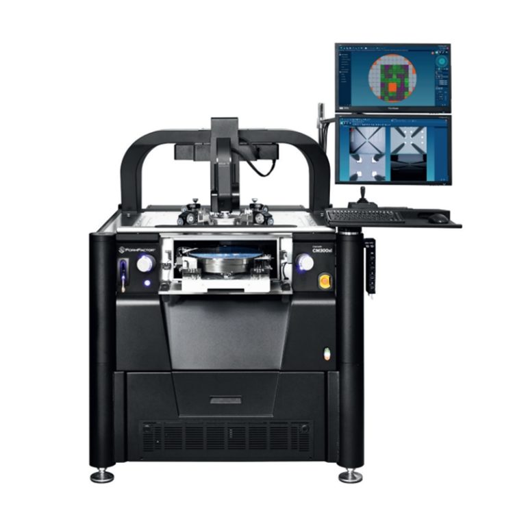
Equipment features: 1. Non-destructive precision testing Micrometer-level probe contact technology (minimum...
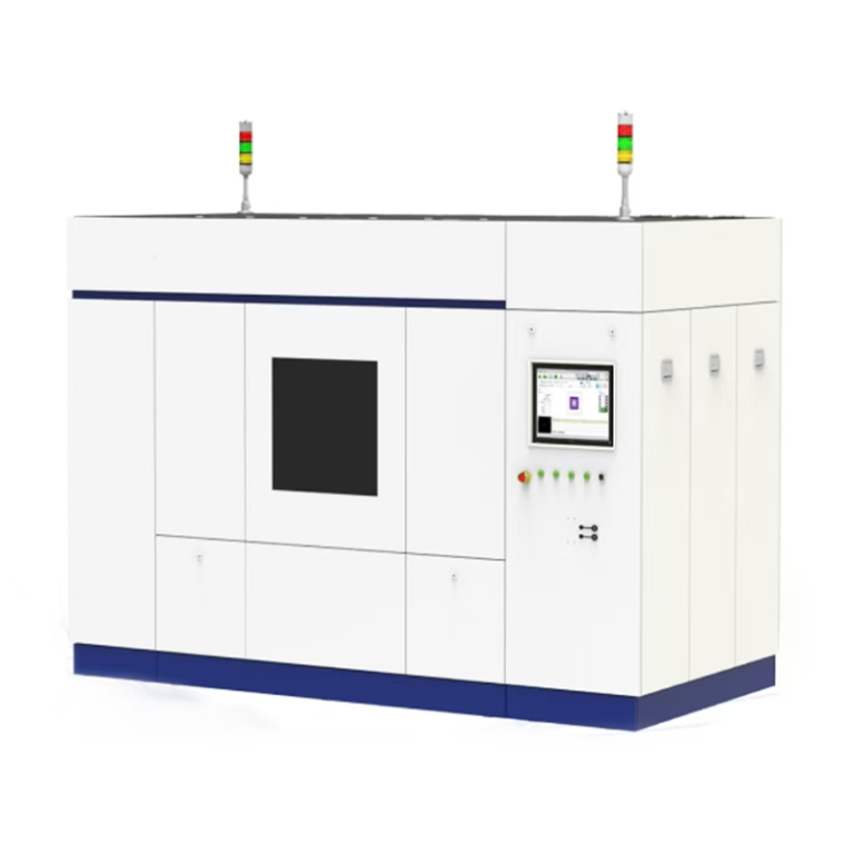
Equipment features: 1. Using maskless direct writing lithography technology, high-precision electron...
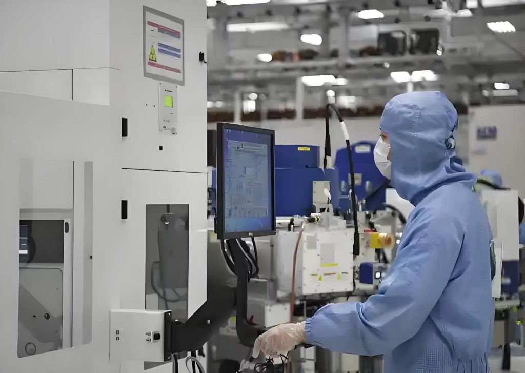
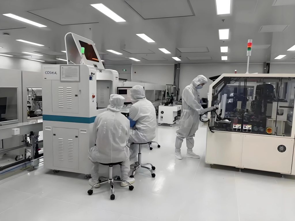
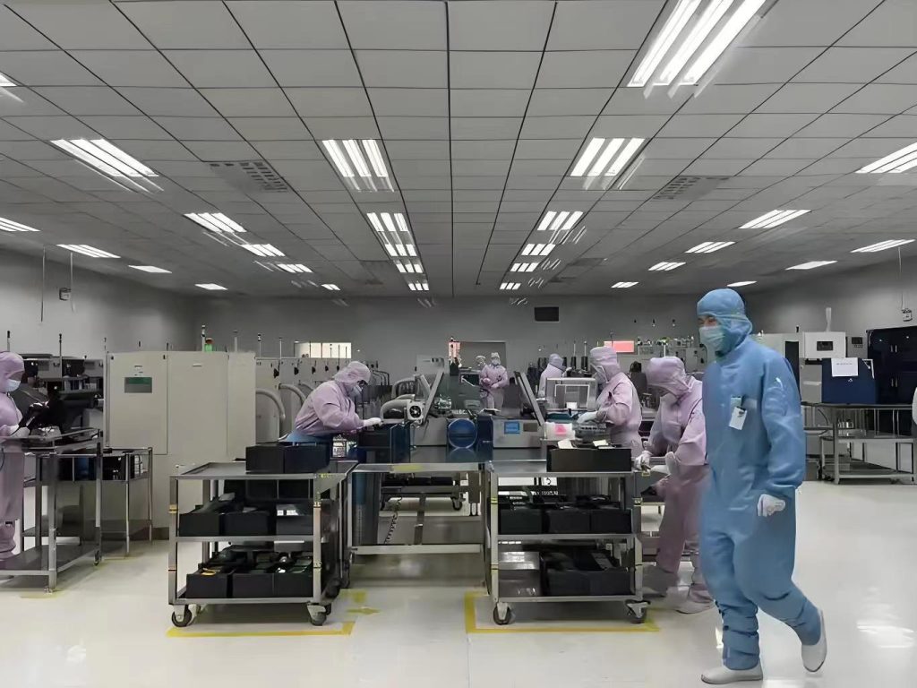

Title: Semiconductor manufacturing processes Objective: To have a certain foundation for the overall...


