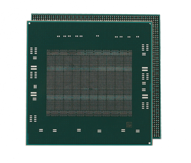
Material composition
- Core materials
Pure copper (CU): high thermal conductivity (~ 400 W/M·K), high electrical conductivity, but high thermal expansion coefficient (~17 x 10⁻⁶/K).
Copper alloy (CU-MO, CU-W): reduce the coefficient of thermal expansion (CTE), improve mechanical strength, but slightly lower thermal conductivity.
- Insulation layer material
Epoxy resin (FR-4): low cost, but poor thermal conductivity (~ 0.3 W/M · K).
Ceramic filled epoxy (such as AL₂O₃, ALN filled): improve thermal conductivity (1-5 W/M·K).
Direct copper cladding (DBC, DIRECT BONDED COPPER): alumina (AL₂O₃) or aluminum nitride (ALN) ceramic copper cladding with higher thermal conductivity (24-200 W/M·K).
- Surface treatment materials
Chemical nickel/gold plating (ENIG): improves oxidation resistance and welding properties.
OSP (organic solderable protective film): low cost oxidation protection scheme.
- Substrate pretreatment: copper foil surface cleaning (acid washing, micro etching) to enhance adhesion.
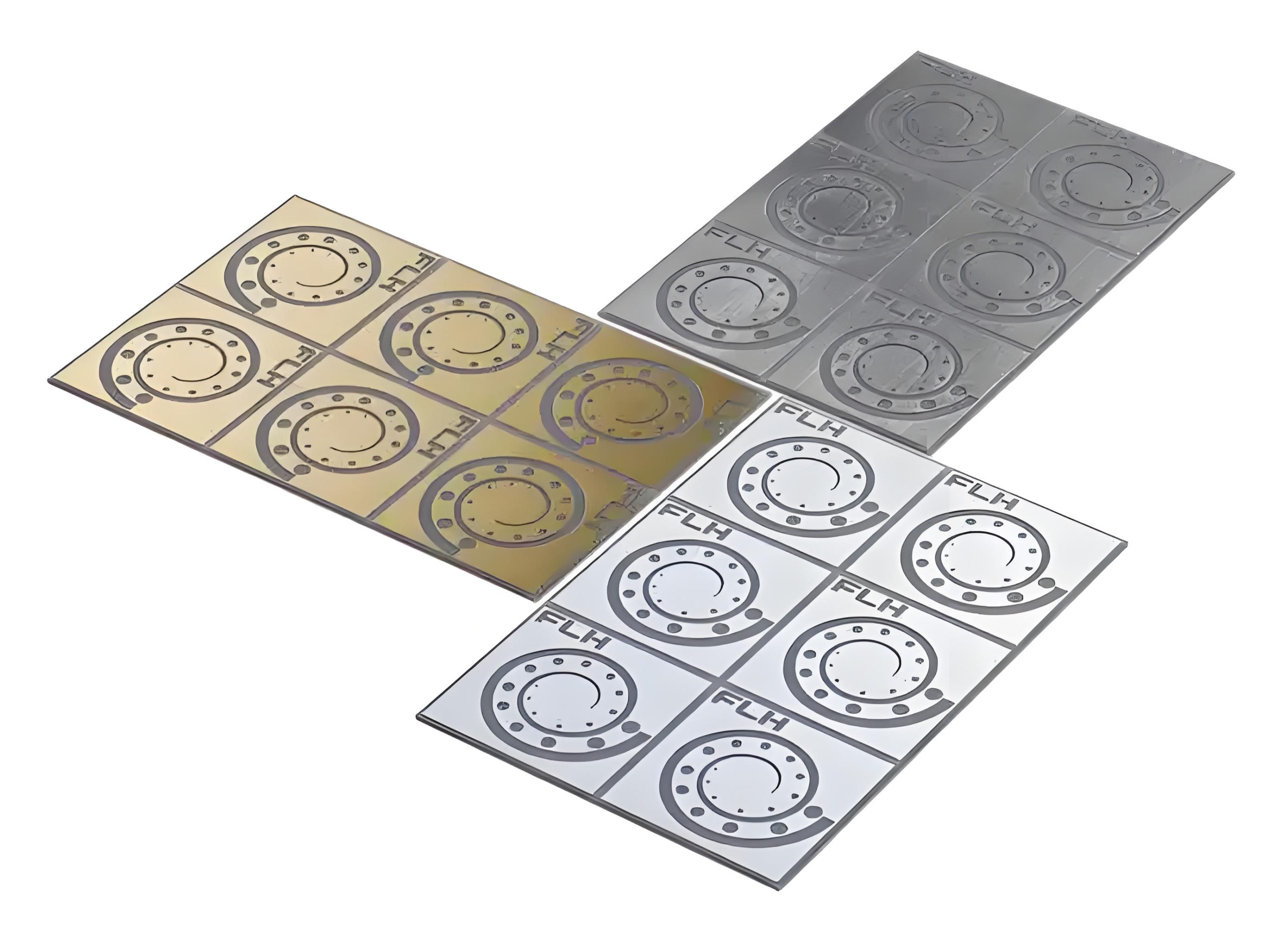
- Graphical:
Dry film lithography: LDI (laser direct imaging) technology is used to achieve 10ΜM line width accuracy.
Acid etching: FECL₃ etching solution, control side etching rate <15%.
- Insulation layer formation:
Ceramic substrate: direct copper coating (DBC) process is used, and the copper and AL₂O₃ are eutectic bonded at 1065℃.
Resin substrate: vacuum pressing (pressure 15-30KG/CM², temperature 180℃) to avoid bubbles.
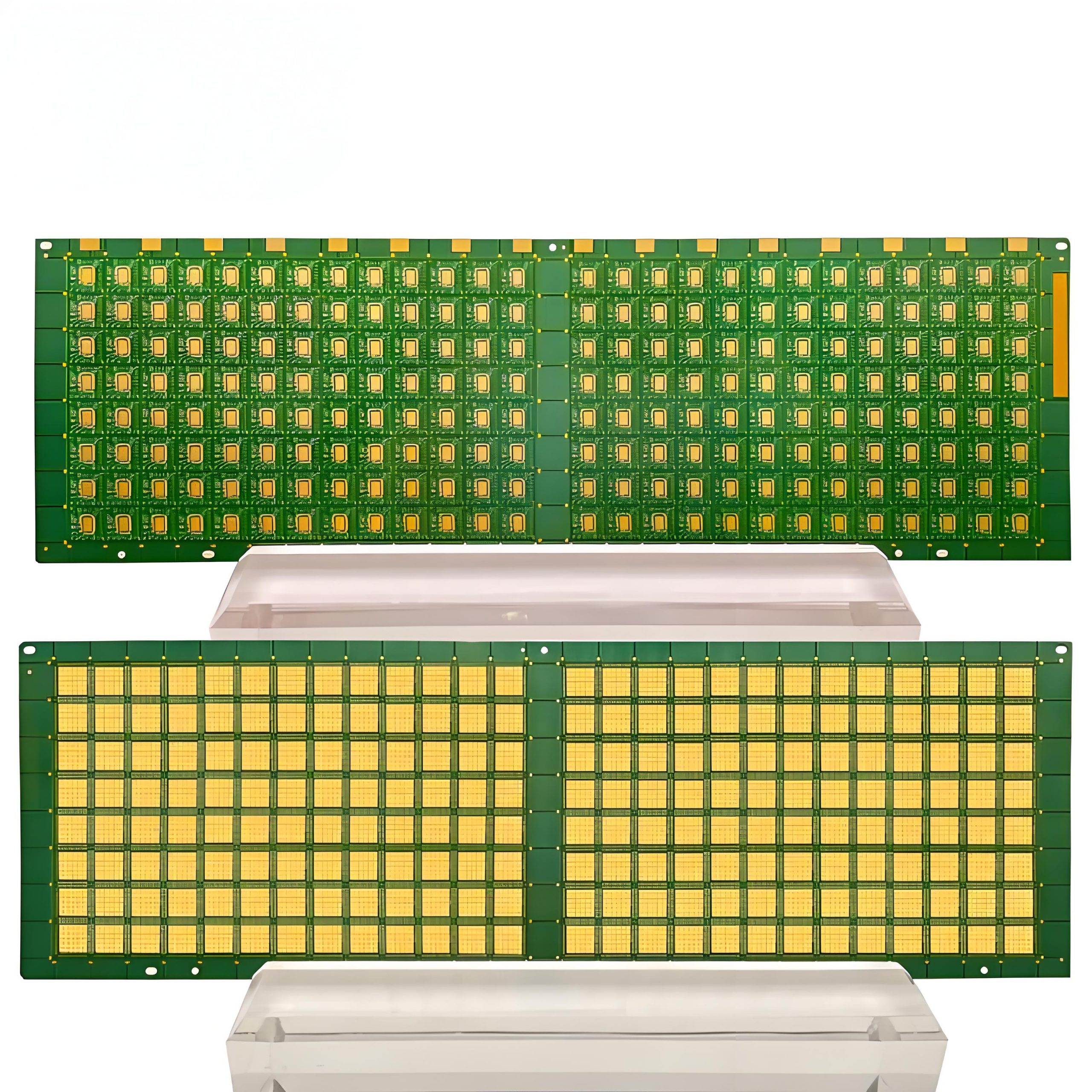
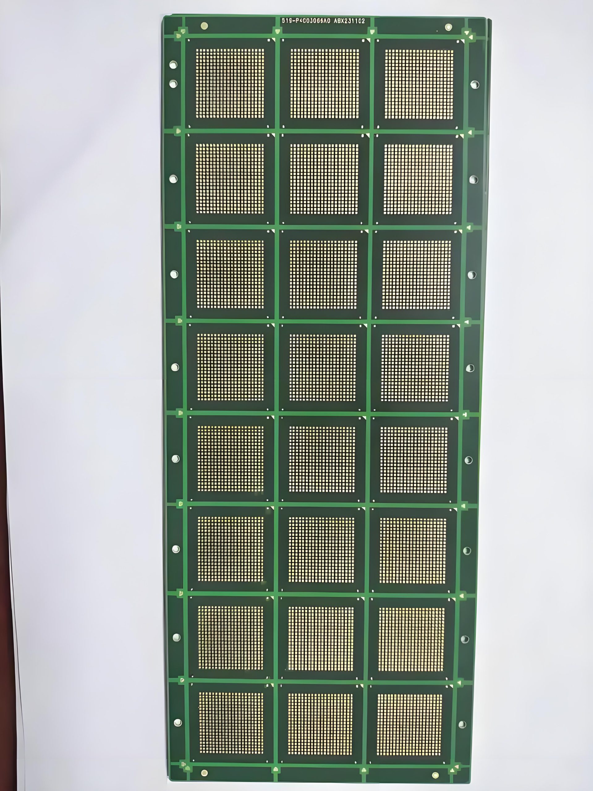
- Drilling and metallization:
Laser drilling (CO₂ laser, aperture 50-150ΜM).
Chemical copper plating (thickness 1-2ΜM) + electroplating thickening (20-30ΜM).
- Surface treatment:
ENIG (chemical nickel gold): nickel layer 3-5ΜM, gold layer 0.05-0.1ΜM.
Antioxidation treatment: OSP film thickness 0.2-0.5ΜM.
- material performance advantages
| function | Copper substrate (DBC/AMB) | Traditional FR-4 PCB | Ceramic substrate (AL₂O₃/ALN)
| Thermal conductivity (W/M·K) | pure copper 398 W/M·K, DBC substrate can reach 370 W/M·K | 0.3-5 (MCPCB) | 24-200 (ALN)
| Thermal expansion coefficient (×10⁻⁶/K) | 6-8 (DBC) | 14-18(FR-4) | 4.5-7(ALN)
| mechanical strength | tall | same as | tall
High temperature resistance | High (DBC/AMB) | Low (<150°C) | Very high (>1000°C)
| prime cost | higher | low | tall
core advantage:
✅ Superior thermal conductivity (better than traditional PCB, close to ceramic substrate)
✅ Low coefficient of thermal expansion (CTE) (suitable for semiconductor chips to reduce thermal stress)
✅ High current carrying capacity (high conductivity of copper)
✅ High temperature resistant and heat shock resistant (DBC/AMB can withstand>300°C)
- Industry application and technical index advantages
- Power semiconductors (IGBT, SIC/GAN modules)
High thermal conductivity (>100 W/M·K) reduces junction temperature and improves device life; low CTE (6-8×10⁻⁶/K) matches SI/SIC chips and reduces thermal stress cracking. Suitable for electric vehicle inverters, industrial frequency converters, photovoltaic inverters.
- LED packaging (high power LED, COB packaging)
High efficiency heat dissipation, improve LED light efficiency and life, copper high reflectivity can improve LED light output efficiency, suitable for car headlights, outdoor display screens, plant lighting.
- RF/microwave devices (5G base stations, radar)
Low dielectric loss (DBC ceramic insulation layer), suitable for high frequency applications, copper’s high conductivity reduces signal loss, suitable for 5G PA module, military radar, satellite communication.
- Automotive electronics (electric drive, BMS, on-board charging)
High temperature resistance, vibration resistance, suitable for harsh vehicle environment, high current carrying capacity, suitable for high power electric drive system, suitable for electric vehicle motor controller, battery management system (BMS).
New energy vehicles: 800V SIC inverter module (such as Tesla MODEL 3 rear drive module).
5G communication: MASSIVE MIMO AAU power amplifier (Huawei32T32R equipment).
Aerospace: Starborne phased array radar T/R components (temperature resistant-196℃ ~ +200℃).
Industrial power supply: 10KV/1000A IGBT crimping package.
- Future development trends
Material innovation:
Nano composite copper (strength increased by 50%, thermal conductivity maintained at 95% purity level).
Gradient CTE design (copper/molybdenum/copper sandwich structure, CTE 7 PPM/℃).
Process upgrading:
The half addition method (MSAP) achieves 3ΜM line width and is suitable for GAN MMIC.
Low temperature co-fired copper (LTCC) technology, sintering temperature <300℃.
Emerging applications:
Quantum computing superconducting circuit (RF performance optimization of copper substrate at 10MK).
First wall material of fusion reactor (copper/tungsten lamellar structure, resistant to 10 MW/M² heat flow).
Copper substrates, with their superior thermal and electrical conductivity and continuous technological innovation, have become the preferred choice for high-power density electronic systems. It is projected that the global copper substrate market will exceed $2.8 billion by 2025, with a CAGR of 12.3%. As wide-bandgap semiconductors, 3D integration, and nanomaterials advance, copper substrates will continue to evolve towards higher thermal conductivity, lower CTE, and greater environmental friendliness, becoming the cornerstone of next-generation electronic packaging


