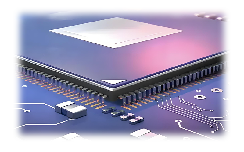
- Miniaturization and high density
Compact design: 5070% less PCB area than traditional DIP package, with pin spacing typically 0.651.27MM.
Thin and light: the thickness can be controlled at 1.02.0MM, suitable for space limited scenarios (portable medical devices).
- Excellent electrical properties
Low parasitic parameters: short lead frame design reduces inductance (<2NH) and supports high speed signal transmission (>500MHZ).
Insulation of ceramic: dielectric constant 910 (1MHZ), suitable for high frequency mixed signal circuits.
- High reliability and environmental tolerance
Air tight packaging: glass/metal seal, leakage rate <1×10⁻⁸ ATM·CC³/SEC, MILSTD883 certified.
Wide temperature operation: 55°C to +200°C, resistant to humidity and heat, salt spray corrosion (marine equipment application).
Anti-mechanical impact: The ceramic structure has excellent vibration and bending resistance, suitable for vehicle or industrial vibration environment
- Thermal management capability
Thermal conductivity of ceramic: the thermal conductivity of AL₂O₃ substrate is 2030 W/M·K, and metal heat sink (copper alloy) can be integrated
- Key technical indicators in industrial applications
| qualification | Typical values/characteristics | Application impact
| Pin count / spacing | 832 pins, spacing 0.51.27MM | Medium complexity IC packaging (MCU, memory)
| Signal complete | The transmission rate is 5 GBPS | Insertion loss <0.3 DB @ 5 GHZ
| Thermal resistance (RTH) | 1530°C/W (depending on substrate material) | Supports the stable operation of 510W power devices
| frequency response | DC~3GHZ | Medium and high speed data communication, RF front end module
| Air tightness grade | Helium leak rate <1×10⁻⁸ ATM·CC³/SEC | Long-term reliability of medical implants and aerospace equipment
| mechanical strength | Bending strength> 150MPA | Vehicle-mounted electronic vibration resistance requirements
- Typical application scenarios
- Consumer electronics and communication equipment
Smartphone RF front end: Compact packaging requirements for 5G millimeter wave bands (28/39 GHZ).
Optical module transceiver: high frequency signal transmission and low loss characteristics are suitable for high speed optical communication (100G PAM4).
- Automotive electronics
ADAS control unit: Camera/radar signal processing chip, resistant to vehicle temperature shock (40°C to +125°C).
Vehicle information and entertainment system: high-density integration to meet the miniaturization requirements of the central control screen driver IC.
- Industrial and medical equipment
Industrial sensor module: corrosion resistant ceramic is suitable for chemical industry, oil and gas exploitation and other harsh environment.
Portable medical devices: ultra-thin packaging for low-power chips such as blood glucose meters and electrocardiogram monitors.
- Ultra-thin and high density
Thickness breakthrough: Develop ultra-thin ceramic substrates below 0.5MM to accommodate foldable devices and micro-sensors.
3D stack integration: multi-layer interconnection is achieved through TSV (silicon through-hole) technology to improve I/O density (number of pins>100).
- Material and process innovation
Aluminum nitride ceramics are popularized: thermal conductivity is increased to 170 W/MK, supporting higher power chips (GAN devices).
Low temperature co-fired ceramics (LTCC): integrated passive components (inductor/capacitor), simplifying peripheral circuit design.
- Intelligence and green manufacturing
AI-assisted design: Machine learning optimizes heat distribution and pin layout to reduce development cycle and cost.
Environmental protection process: lead-free welding and recyclable ceramic materials are used, in line with ROHS/REACH standards.
- Expansion of emerging areas
Internet of Things (IOT) devices: ultra-low power chip packaging for smart home and wearable devices.
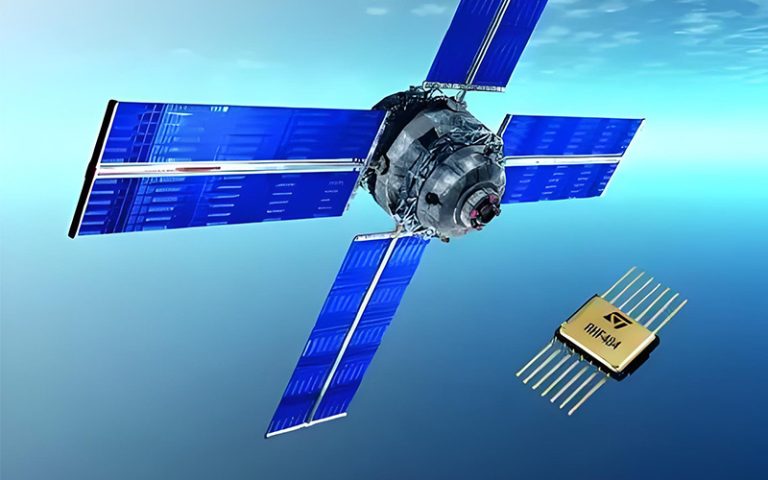
Microsatellite (CUBESAT): Lightweight, radiation-resistant ceramics to meet the electronic needs of low-cost satellites.
CSOP, with its miniaturization, high reliability, and superior electrical performance, is widely used in consumer electronics, automotive, and medical fields. In the future, as the demand for 5G, IoT, and miniaturization grows, CSOP will further penetrate emerging areas such as wearable devices and smart sensing through ultra-thin design, material innovation (aluminum nitride), and 3D integration technology, becoming a core solution for high-density electronic system packaging.


