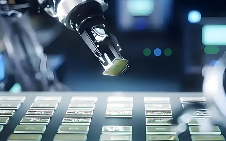
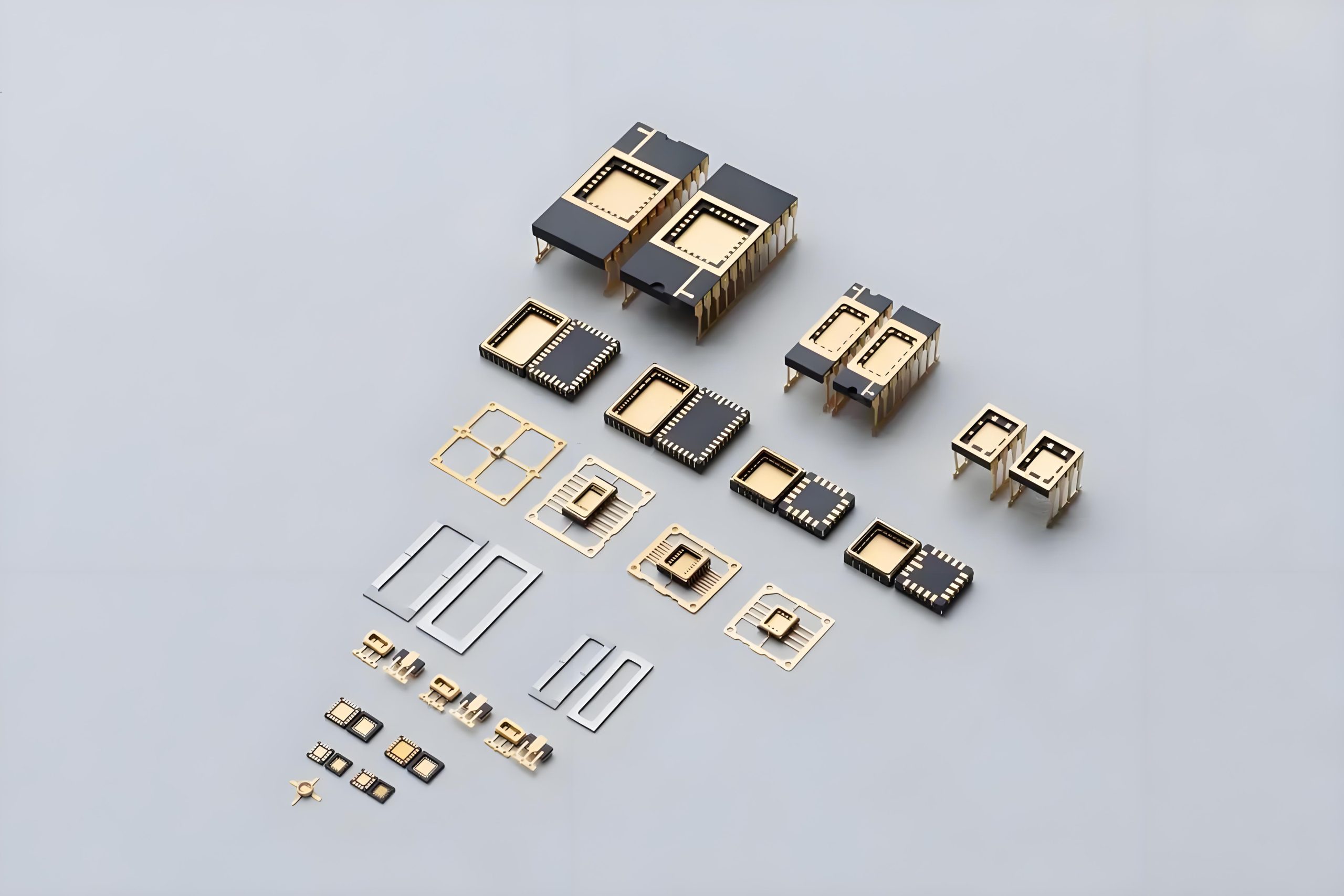
Core advantages of CLCC
- Ultra-reliable design
Full ceramic gas sealed: glass or metal solder sealed, leakage rate <1×10⁻⁸ ATM·CC³/SEC, moisture-proof and corrosion-resistant, MILSTD883 certified.
No lead structure: eliminate the mechanical stress problem of traditional pins, and improve the vibration resistance by more than 50%.
- Advantages of high frequency and high speed signals
Low parasitic parameters: The pinless design makes the inductance <0.5NH, supporting high frequency applications (up to 20GHZ), 5G millimeter wave module.
Dielectric properties of ceramic substrate: dielectric constant (DK) 910, loss Angle (TANΔ) <0.001, better than organic substrate.
- Compact thermal management
Bottom metal pad: directly weld the PCB heat dissipation layer, thermal resistance as low as 815°C/W (ALN substrate can reach 5°C/W).
High temperature resistance: working temperature 55°C to +200°C, short term can withstand 300°C reflow soldering.
- Miniaturization and lightweight
Size reduction: 30% more space than QFN, typical size 5x5MM to 40x40MM, thickness 1.04.0MM.
Very light weight: ceramic density 3.54.0G/CM³, suitable for aerospace equipment.
- Prominent technical indicators in industrial applications
The key technical indicators of CLCC define its competitiveness in the high-end field:
| qualification | Typical values/characteristics | Application impact
|I/O quantity | 16100+ pads (peripheral or array layout) | medium to high complexity IC packaging (RFIC, MCU)
| Thermal resistance (RTH) | 515°C/W (ALN substrate optimized <5°C/W) | Supports 1030W high power density devices
| frequency response | DC~20GHZ+ | Millimeter wave radar, satellite communication front module
| Air tightness grade | Helium leak rate <1×10⁻⁸ ATM·CC³/SEC | Ensure the life of aerospace/medical equipment for more than 10 years
| mechanical strength | Bending strength> 200MPA | Demand for electronic resistance to mechanical shock in vehicles
- Typical application scenarios
- High frequency communication and optoelectronics
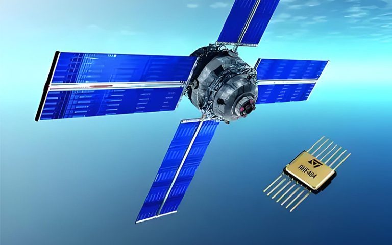
5G base station RF module: supports millimeter wave band (28/39 GHZ) signal transmission, suitable for high frequency low loss requirements.
Optical communication transceiver: laser and detector packaging for 100G/400G optical modules to ensure high-speed signal integrity.
- Aerospace and defense industry
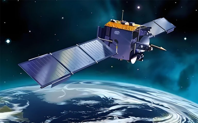
Satellite payload control unit: radiation resistant ceramic is adapted to the space environment (total dose radiation>100 KRAD) to ensure long-term stability.
Missile guidance system: withstands mechanical shock and temperature change during high speed flight.
- Industrial and medical equipment
Industrial sensor module: corrosion resistant ceramic is suitable for chemical, oil and gas exploitation and other harsh environment, high temperature pressure sensor.
Implantable medical devices: long-term airtightness to ensure the reliability of chips in devices such as pacemakers (life>30 years).
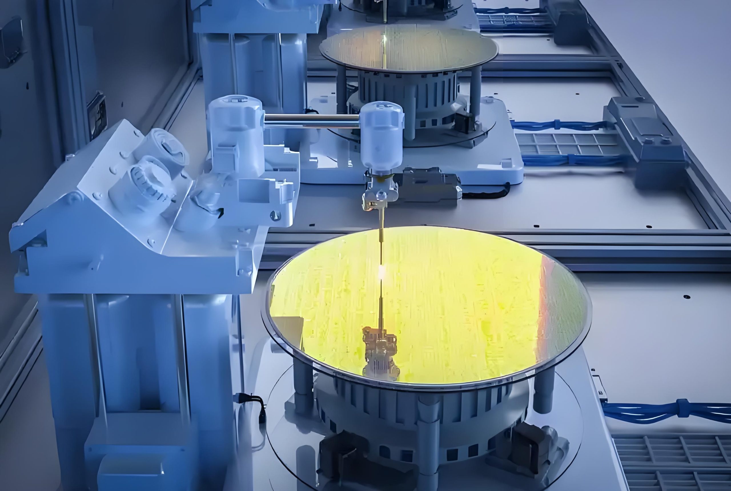
- Material innovation and performance upgrade
Aluminum nitride ceramics are popular: replacing alumina, the thermal conductivity is increased to 170 W/MK, and the thermal resistance is reduced to less than 10°C/W, suitable for high power density chips (GAN devices).
Composite structure design: ceramic metal composite substrate combines the advantages of both sides to improve mechanical strength and heat dissipation efficiency.
- Integration and multifunctionality
3D stacking technology: multi-layer ceramic substrate vertical interconnection is realized through TSV (silicon through-hole), passive components are integrated (LTCC technology), and peripheral circuit volume is reduced.
Heterogeneous packaging (SIP): integrated with optoelectronic devices and MEMS sensors, and expanded to optical communication modules and intelligent sensing fields.
- Intelligence and green manufacturing
AI-driven process optimization: machine learning to optimize sintering parameters and thermal field distribution to improve yield and reduce energy consumption.
Application of environmental protection materials: lead-free welding process and recyclable ceramic materials are developed to meet ROHS/REACH standards.
- Expansion of emerging areas
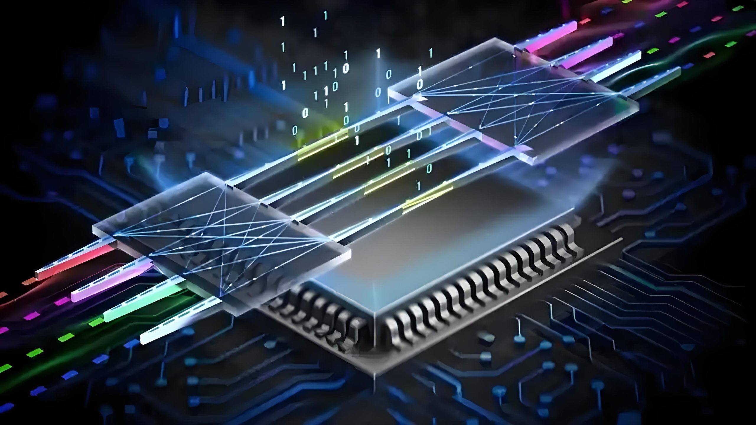
Quantum computing cryogenic packaging: the extremely low temperature environment (below 4K) suitable for superconducting qubits requires the design of cryogenic compatible materials.
Internet of Things and Wearable Devices: Ultra-thin CLCC packaging (thickness <0.8MM) is used for smart wearable sensors to support low power consumption and miniaturization requirements.
c


