Chemical Vapor Deposition (CVD) and Physical Vapor Deposition (PVD) are key methods for creating thin films in chip-making and special coatings. CVD uses gases that react on a hot surface to make a solid layer. It’s great for covering tricky shapes and controlling the film’s makeup. PVD uses simple processes like blasting or heating materials to stick them to a surface. It’s easier and works with many metals, but struggles with complex shapes. CVD makes dense, sticky films and precise layers, while PVD is quicker and works with more materials. DEEPETCH builds advanced CVD tools that improve film evenness and work well for chips and tiny machines. New ideas like atomic-layer CVD and smart computer controls are making these tools even better. Choosing between CVD and PVD depends on what you need for your projects, like shape coverage, material type, and cost.
What Are the Core Differences Between Physical and Chemical Deposition Methods?
Thin film methods are vital for making chips, tiny machines, light-based devices, and tough coatings. You’ll often see two main ways: Chemical Vapor Deposition (CVD) and Physical Vapor Deposition (PVD). They differ in how they work, what tools they need, and how well they perform.
How Do Physical and Chemical Deposition Mechanisms Work Differently?
In CVD, gases mix and react on a hot surface to form a solid layer. This reaction makes films that cover surfaces evenly. Meanwhile, PVD physically moves material from a source to a surface. It might blast atoms off a target or heat material until it turns to vapor.
The big difference is how they interact with the surface. CVD uses heat to spark chemical changes on the surface. PVD relies on physical force or heat without changing the material’s chemistry.
Which Process Parameters Most Influence Deposition Results?
Both methods need careful control of things like:
- Heat
- Pressure
- Gas flow (in CVD)
- Power (in PVD)
For CVD, the chamber’s heat affects how fast reactions happen and how evenly the film is formed. In PVD, the vacuum level and the setup between the material source and the surface matter for good coverage.
The film’s strength, stickiness, grain size, and purity depend on these settings. Adjusting them well helps you get strong films for electronics or coatings for tiny machines.
Why Is Chemical Vapor Deposition Preferred for Complex Structures?
CVD shines at covering complex shapes evenly because it works through surface reactions. It coats deep grooves or holes in 3D chip designs perfectly.
How Do Precursor Chemistry and Chamber Conditions Affect Film Growth?
In CVD, special gases flow into a hot chamber. These gases break down or react near the surface to form a solid layer. The type of gas—whether it’s metal-based or another kind—affects how easily it moves, reacts, and keeps the film clean.
The surface needs to be hot enough to start the reaction, but not so hot that unwanted particles form in the air. Chamber pressure matters too. Low pressure helps gases move straight to the surface. Higher pressure helps gases spread into tight spaces for better coverage.
What Are the Key Benefits of CVD for High-Performance Applications?
CVD offers two big perks:
- It covers deep, narrow shapes evenly.
- It makes very clean films because you can control the chemical reactions.
These make CVD great for thin layers in transistors or protective coatings in light-based devices. Also, CVD can work with a method called atomic layer deposition (ALD). This lets you build films one atom at a time, perfect for tiny devices.
How Does Physical Vapor Deposition Compare in Process Characteristics?
PVD is simpler than CVD and works with many materials, like metals that are hard to use in CVD. It’s less fancy but very useful.
What Are the Primary Techniques Within Physical Vapor Deposition?
PVD mainly uses two methods:
- Heating: The material gets so hot that it turns to vapor and sticks to the surface.
- Blasting: A gas beam hits a material source, knocking off atoms that land on the surface.
Both need a super clean, low-pressure environment—around 10⁶ Torr—to avoid dirt and let atoms travel straight to the surface.
Where Does PVD Fall Short in Coating Complex Topographies?
PVD works in a straight line from source to surface. This makes it hard to coat deep grooves or overhangs. Atoms can miss tight spots, causing uneven layers or shadows. You can try rotating the surface or using special tools, but it’s still not as good as CVD for complex shapes.
Which Method Performs Better Across Industrial Metrics Like Adhesion and Cost?
Choosing CVD or PVD depends on balancing film quality, speed, scale, and budget.
How Do Substrate Compatibility and Adhesion Vary Between Techniques?
CVD films stick better because they bond chemically to the surface. This makes them strong against heat changes or physical stress. PVD films might peel off if the surface isn’t prepped well, as they rely on weaker physical bonds.
However, PVD works with more materials, like tough metals, which can be hard for CVD because of gas or heat limits.
What About Film Density and Throughput Efficiency?
CVD films are denser with fewer gaps because they grow atom by atom through careful reactions. This is great for blocking moisture in sensitive devices like screens or sensors.
For speed, CVD tools can coat many surfaces at once with great evenness. But they take longer than PVD systems, which are faster and cheaper to set up.
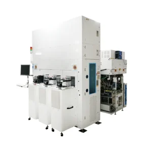
How Does DEEPETCH Enhance Your Precision Manufacturing With CVD Tools?
If you need top-notch thin film solutions for chips or tiny machines, DEEPETCH offers advanced CVD tools built for precise control over tricky shapes.
Why Are DEEPETCH’s Systems Suited for Semiconductor-Grade Materials?
DEEPETCH’s unique gas delivery system spreads gases evenly across surfaces, even during long processes. This ensures consistent films. Whether you’re adding silicon nitride for protection or special oxides for chip tuning, their tools keep tight control for tiny chip designs.
Their advanced heat controls adjust surface temperatures in real time. This reduces stress or thickness differences across the surface.
Which DEEPETCH Products Excel at Coating High-Aspect Ratio Features?
For deep grooves or holes in memory chips, DEEPETCH’s AL-Chem™ Series uses low-pressure CVD with optional plasma boosts to coat evenly while saving time. These tools handle shapes with extreme depth-to-width ratios—over 50:1—perfect for advanced 3D chip designs.
When Should You Choose One Technique Over Another Based on Application Needs?
Your project’s needs decide whether CVD’s precision or PVD’s flexibility is better. DEEPETCH provides tools for both paths.
For MEMS Fabrication Projects—Which Method Meets Stress Control Demands Best?
Tiny machines need films that don’t bend or break delicate parts. CVD silicon nitride can be tuned with heat to avoid stress, unlike PVD films, which often pull too tightly.
Also, tiny machines have deep cavities. CVD coats these evenly, ensuring sidewalls and bottoms are covered well.
Can DEEPETCH Systems Help Customize Films for Optoelectronic Devices Too?
Yes! Light-based devices need clear conductive layers, anti-glare coatings, or buffer films. DEEPETCH’s CVD tools offer custom recipes to build these without mixing unwanted materials. Their systems have separate chamber zones for clean work.
This lets you control layer thickness precisely for devices like LEDs or light guides in chip-based optics.
What Is Next in Thin Film Technologies That Could Impact Your Workflow?
Thin film tech is moving toward super-precise layers and smart automation.79 This will change how you build tiny devices at large scales.
Is Atomic Layer Chemical Vapor Deposition Becoming Mainstream?
Atomic layer CVD (ALCVD) builds films one layer at a time by cycling reactions. This gives exact control over thickness, crucial when errors must stay under 1 nanometer. DEEPETCH’s ALChem™ tools support this with clean, metal-based gases for ultra-fine layers.
ALCVD also fills deep shapes better than regular CVD by coating surfaces step-by-step. It’s ideal for 3D memory chips where vertical designs are key.
Will AI-Based Process Optimization Improve Yield Consistency Across Batches?
Yes! DEEPETCH uses smart computer programs trained on past process data. These predict problems before they hurt output. By tweaking pressure or heat automatically based on live feedback, you get steady results with less manual work.
FAQ
Q1: What makes Chemical Vapor Deposition better suited than physical methods for coating complex geometries?
A: CVD uses surface reactions, not straight-line paths like PVD. This lets it cover deep grooves and sharp corners in advanced chip designs evenly.
Q2: Can I deposit metals using Chemical Vapor Deposition?
A: Yes, but you need special metal gases that break down cleanly. This is trickier than PVD, which easily blasts metals onto surfaces.
Q3: How does DEEPETCH help improve thin film uniformity across large substrates?
A: Their tools use smart gas flow and zoned heating to keep gases and heat even across big surfaces, even for thick layers.


