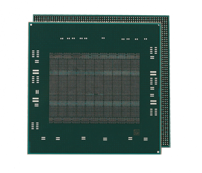
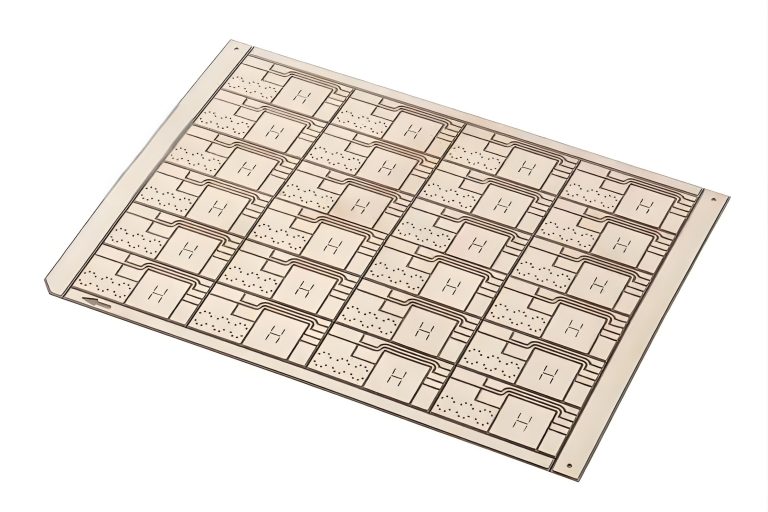
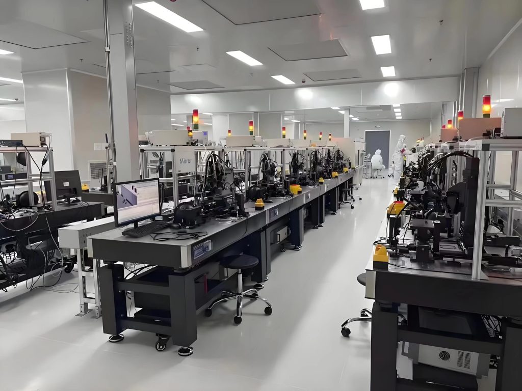
Product Introduction
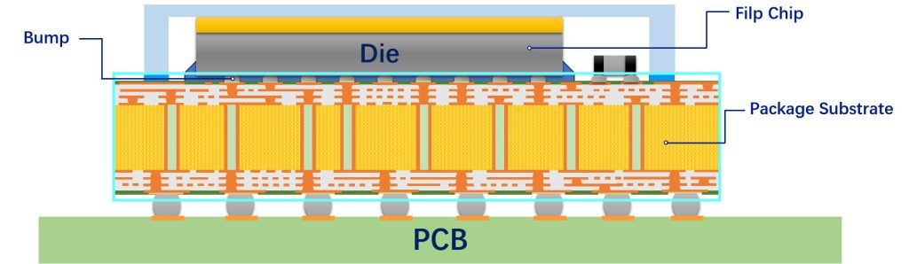
The products generally adopt the Build-up Film Lamination process, and the circuit formation uses the semi-addition (SAP) process. The representative products include the FCBGA(Flip Chip Ball Grid Array) packaging in the form of flip-chip packaging
Features of this type of product: large size, high multi-layer, high density; It is used for applications with high computing power (HPC), such as GPU, CPU, FPGA, AI computing, 5G/6G and other scenarios.
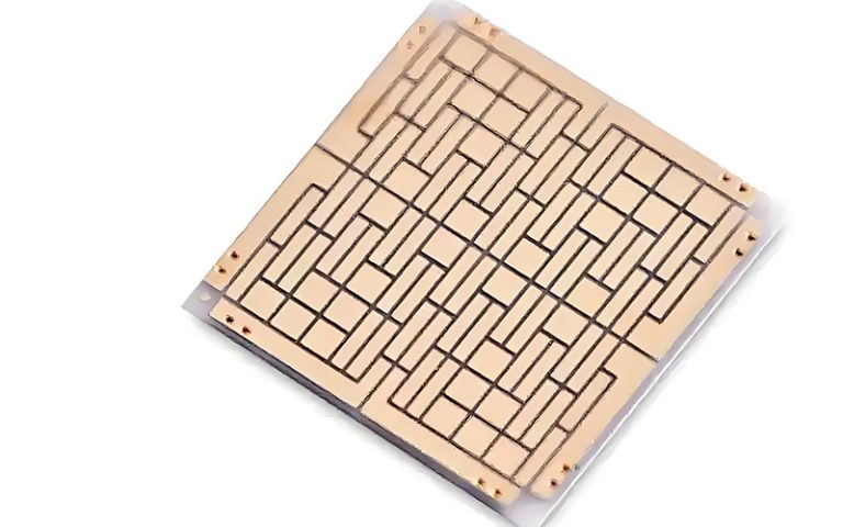
Package Structure
Features
|
Smaller micro via by new-generation laser drilling machine |
Fine Line/Space by SAP process |
|
Multi-Layer |
Large Unit Size |
High Density |
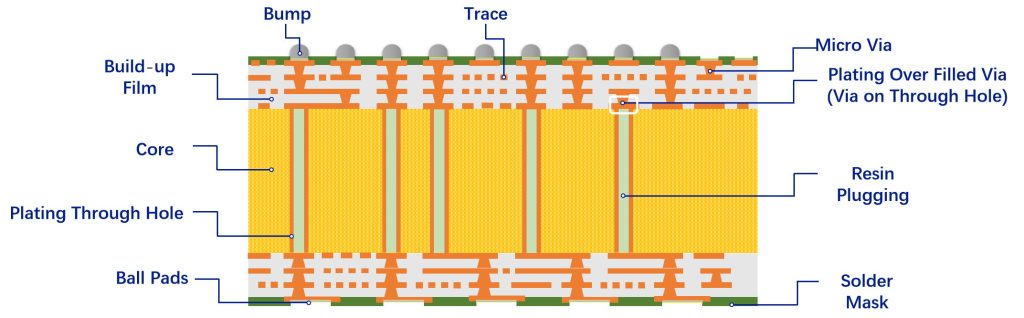
Build-up Structure
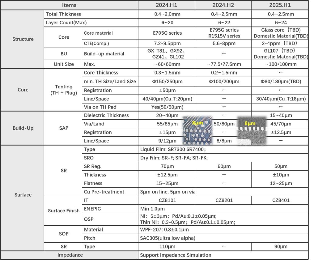
Process Capability
| Process Capability | Applications | |
| · Layer Count | · 6~20 | · CPU、MPU |
| Board Thickness | · 0.2~2.0mm | · GPU |
| · Line/Space | · 9/12μm | · ASIC |
| · Via/Land | · Φ55/85μm | · FPGA |
| POFV(Plating over Filled Via, Via on through hole) | · AI | |
| · SRO | · Φ60μm | · 5G |
| · SRO/Land Reg | · ±12.5μm | · |
| · Surface Finish | · IT、ENEPIG、OSP | · |
| Micro bump Pitch | · 110μm | |
Roadmap-FCBGA
Support FCBGA by BT material: max.16Layers with L/S=12/12um;

Ceramic thin-filmvacuum sensor Optical gas massflowmeter Liquid mass flowmeter Force sensor MEMS...

Photoelectric sensing chip Light source chips Optical transmission and modulationchips Optical detection...

Using a“Detach Core”which has two-layers carrier foil structure on the surface as a core, and forming...
Tenting process is a kind of subtractive process, the process as follows: Laminating photosensitive film...

Modified Semi-Added Process abbreviated as mSAP, which can be used on the core or build-up layers, pattern...

Semi-Added Process abbreviated as SAP, using on the build-up-layer pattern forming as follow:First depositing...
The product generally adopts the pressing lamination process of semi-curing sheets , and line formation...
The products generally adopt the Build-up Film Lamination process, and the circuit formation uses the...
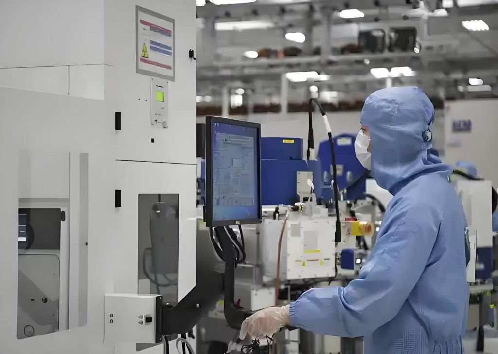
Equipment features: 1. Non-destructive precision testing Micrometer-level probe contact technology (minimum...
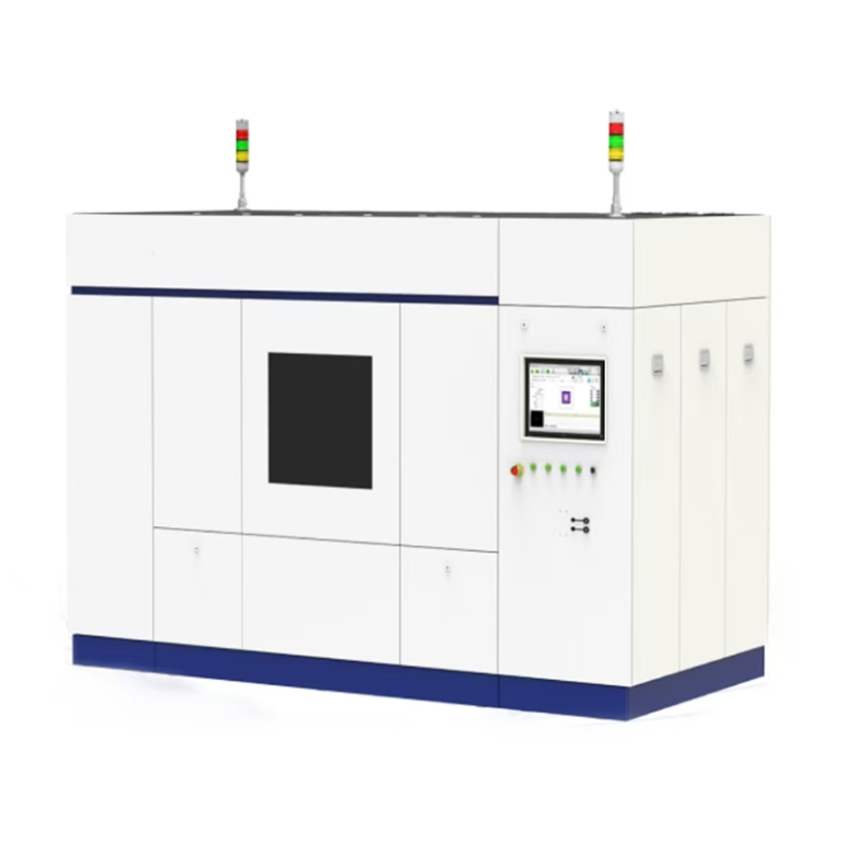
Equipment features: 1. Using maskless direct writing lithography technology, high-precision electron...
Title: Semiconductor manufacturing processes Objective: To have a certain foundation for the overall...


