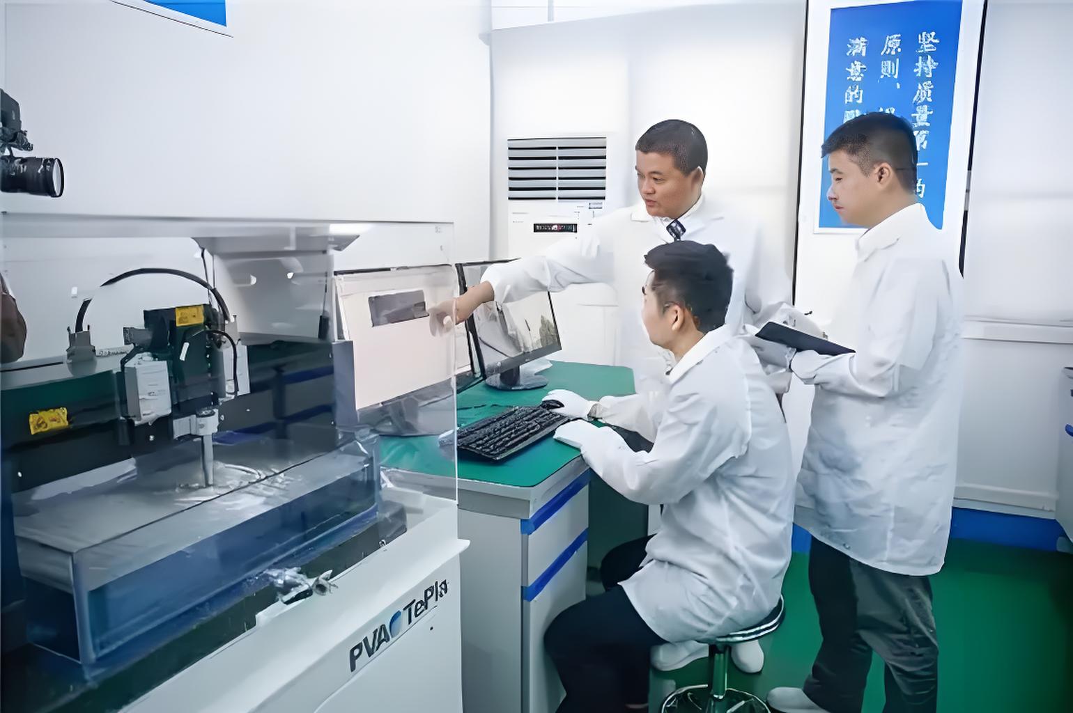
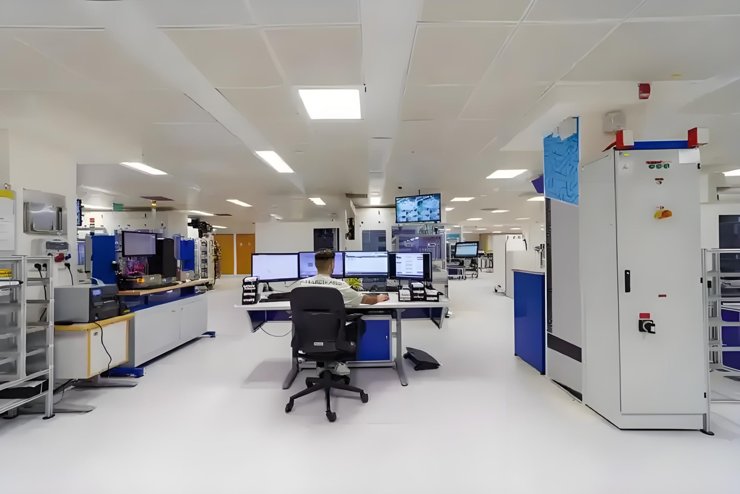
- Manufacturing process of indium phosphide materials
- Material growth technology
Vertical gradient solidification (VGF):
By precisely controlling the temperature gradient growth of single crystal indium phosphide, the dislocation density can be reduced (<500 CM²), the growth cycle is long, suitable for optical communication chip substrate, and suitable for high quality substrate preparation.
Metal organic chemical vapor deposition (MOCVD):
In order to prepare complex heterostructures such as lasers and photodetectors, INP films were epitaxially grown using trimethylindium (TMIN) and phosphine (PH₃) as precursors at high temperature (600-700℃).
Molecular Beam Epitaxy (MBE): In ultra-high vacuum conditions, the interface control accuracy reaches atomic level. High-purity indium phosphide source material is heated and evaporated to form molecular beams, which grow into high-quality indium phosphide single-crystal thin films layer by layer on the substrate. The thickness, doping concentration, and growth rate of the epitaxial layers can be precisely controlled. This process is suitable for nanoscale structures such as quantum wells and superlattices (e.g., INP-based HEMT devices), producing high-quality films with slow growth rates
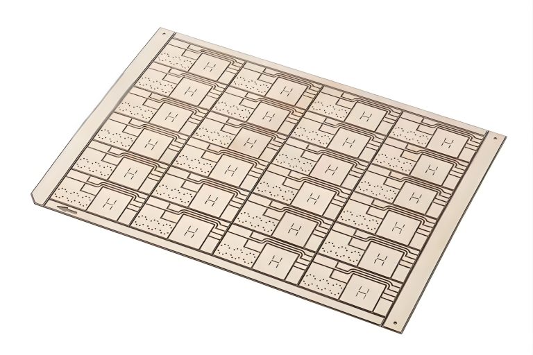
Metal organic chemical vapor deposition (MOCVD): Using metal organic compounds as source materials, chemical reactions are carried out at high temperature to generate indium phosphide thin films. The growth rate is fast, suitable for large area production, and can achieve high uniformity and high repeatability of epitaxial growth.
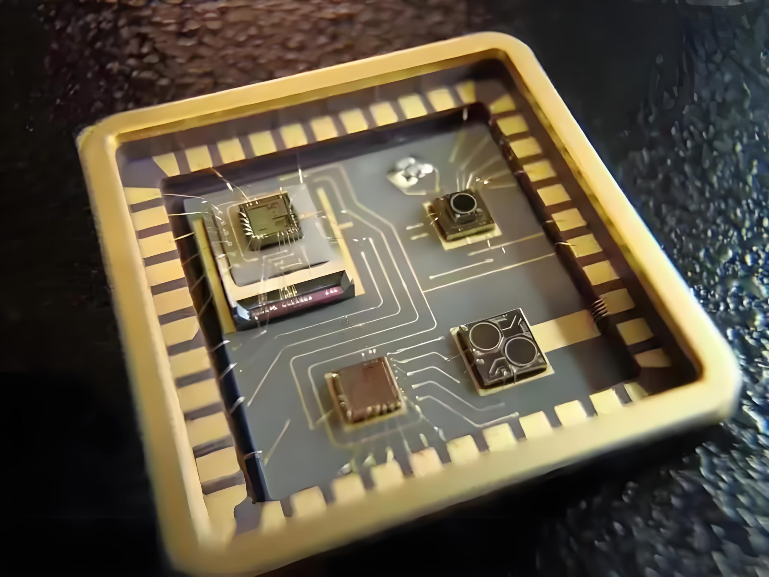
- Core process flow
Substrate preparation:
The INP substrate needs to be polished to a surface roughness <0.2 NM, and the surface state density is reduced by sulfur passivation to improve the reliability of the device.
Doping process:
The carrier concentration can be controlled up to 10¹⁶-10¹⁹ CM⁻³ by doping with silicon (SI) or zinc (ZN).
Lithography and etching:
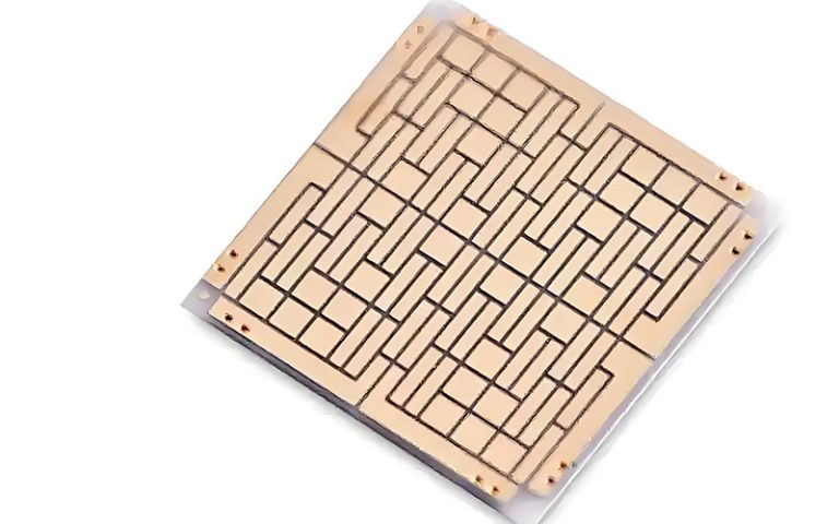
Sub-micron patterning is achieved using electron beam lithography, and waveguide structures (laser resonators) are formed by wet (H₃PO₄:HCL) or dry (ICP) etching.
Passivation and packaging:
The surface is protected by SINₓ or AL₂O₃ passivation layer to reduce dark current (<1 NA in photodetector applications).
- Technical index advantages of indium phosphide
- High frequency and high speed characteristics
Electron mobility: The electron mobility of INP (5400 CM²/VS) is higher than that of gallium arsenide (8500 CM²/VS only in two-dimensional electron gas), but its saturation electron velocity (2.5 x 10⁷ CM/S) is higher, supporting higher frequencies (terahertz band, 0.1-10 THZ).
Thermal conductivity: Thermal conductivity (68 W/M·K) is better than GAAS (55 W/M·K), suitable for high power density devices (power amplifier).
Saturation electron drift velocity: about 1.5 x 10⁷ CM/S, better than gallium arsenide, suitable for high power microwave devices
- Excellent photoelectric performance
Direct band gap (1.35 EV):
Corresponding to 1550 NM communication wavelength, it is the core material of the lowest loss window of optical fiber communication and used in high-speed laser (>100 GBPS) and avalanche photodiode (APD).
High quantum efficiency:
The photoelectric conversion efficiency is> 90% (INGAAS/INP detector), far exceeding that of silicon-based devices.
- Radiation resistance and temperature adaptability
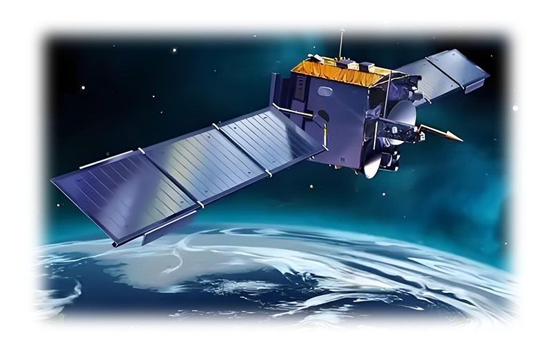
The radiation resistance is better than silicon and GAAS, suitable for aerospace electronic devices (satellite communication payload).
The wide operating temperature range (-200℃ to +300℃) is suitable for deep space exploration and high temperature environment sensors.
- Low noise and high linearity
The noise factor (less than 0.5 DB@10 GHZ) and linearity of INP HEMT are better than GAN and GAAS, making it an ideal choice for millimeter wave radar and 6G communication.
- Core application areas of indium phosphide
- Optical communication and laser technology
1550 NM laser: the core light source of optical fiber communication backbone network and 5G pretransmission network, supporting single-mode output power>100 MW. It can be used to manufacture various optoelectronic devices with high photoelectric conversion efficiency and high sensitivity, suitable for optical fiber communication system and optical display technology.
Quantum computing and lasers: Indium phosphide quantum dots have adjustable emission wavelengths suitable for quantum communication and quantum computing, and narrow linewidth (<100 KHZ) characteristics are suitable for quantum communication and optical communication systems
Optical communication field: mainly used to manufacture optical module devices, such as semiconductor lasers, optical detectors, etc. Support high-speed, large-capacity data transmission.
- High frequency electronic devices
Terahertz imaging and communication: INP-based HEMT and RTD (resonant tunneling diode) can generate and detect 0.3-3 THZ signals for security imaging and 6G ultra-high-speed wireless communication.
Millimeter wave integrated circuits: power amplifier chips for vehicle-mounted radar (77 GHZ) and satellite communications (KA band).
High frequency and high speed applications: High electron mobility (3000-4500 CM²/ (V·S) and high saturation electron drift velocity make it advantageous in the manufacturing of RF devices, suitable for the production of high-end RF devices, RF power amplifiers, high-frequency oscillators, etc., widely used in radar, satellite communication and other fields.
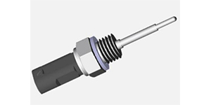
Sensors: Sensors made of indium phosphide have high sensitivity and high precision, suitable for biomedical signal detection and environmental monitoring in wearable devices, medical devices and other fields.
- Photoelectric detection and sensing
APD and PIN detectors: used in lidar (LIDAR) and fiber optic sensing systems with detection sensitivity of-30 DBM.
Gas sensor: The INP based photonic crystal sensor can detect trace gases (methane, CO₂) at the PPB level.
- Future development direction
- Heterogeneous integration technology:
Develop INP-ON-SI or INP-ON-SIC heterogeneous integration scheme to reduce substrate cost and improve heat dissipation capability.
- Application of quantum technology:
The INP quantum dots are used to realize single photon sources and qubits, which promote quantum computing and encrypted communication.
- Wafer size upgrade:
Transition from 4-inch to 6-inch wafers to improve production efficiency and yield (target>80%).
Indium phosphide, through advanced crystal growth techniques and process optimization, boasts high-frequency, high-speed, and high-sensitivity characteristics, making it irreplaceable in optical communication, terahertz technology, and quantum fields. Despite its higher production costs, its irreplaceability ensures a critical role in high-end chip manufacturing. In the future, it is expected to expand its scale application in autonomous driving, 6G communications, and quantum computing through hetero-integration and process optimization.


