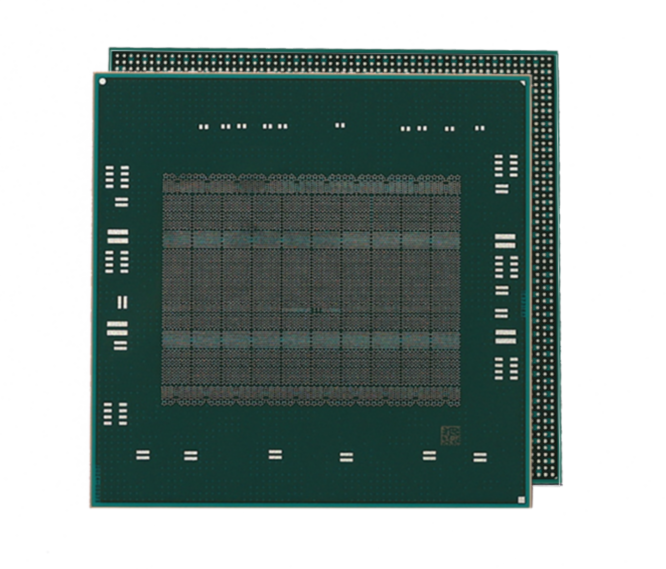
- The material of the glass wafer
The core material of glass wafer is quartz glass (SIO₂), with a purity of 99.9999% or more (6N grade). The electrical and optical properties can be improved by controlling impurities (such as metal ions, hydroxyl groups). Depending on the application requirements, you can choose:
Synthetic quartz glass: prepared by chemical vapor deposition (CVD), with very low hydroxyl content (<10 PPM), suitable for high frequency devices.
Molten quartz glass: natural quartz sand is formed after high temperature melting, the cost is low, suitable for optical or insulating substrate.
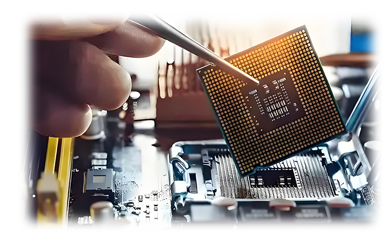
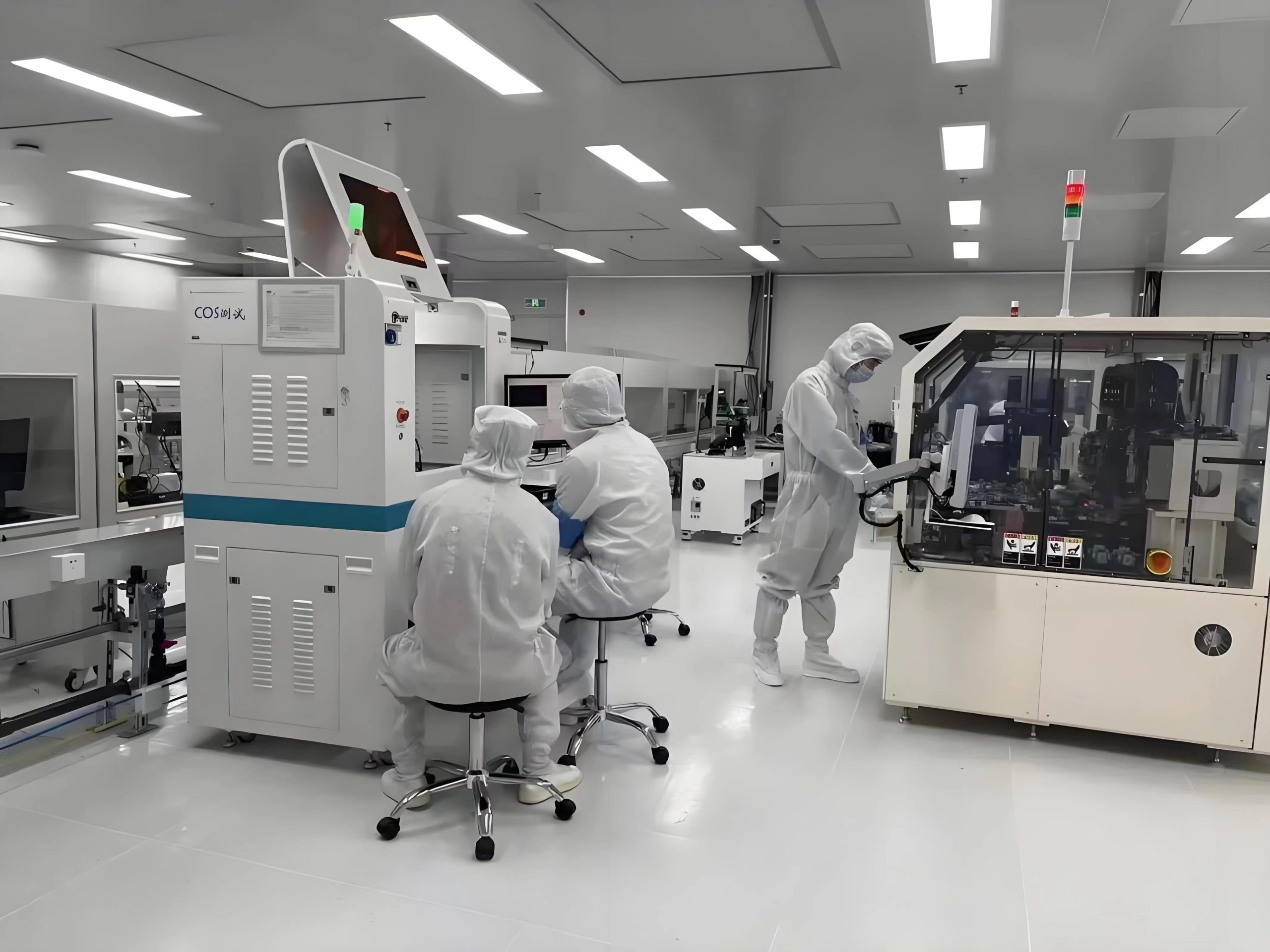
- The manufacturing process of glass wafers
- Raw material preparation
High purity SIO₂ synthesis:
Chemical vapor deposition (CVD): silicon tetrachloride (SICL₄) and oxygen (O₂) are used as raw materials, and SIO₂ particles are generated in high temperature (1500-2000℃) in hydrogen and oxygen flame, and then sintered to form transparent glass body.
Purification of natural quartz: natural quartz sand is removed from metal impurities by acid immersion, flotation and other processes, and the purity can reach more than 99.99%.
- Wafer molding
Drawing or pressing: the molten quartz glass is formed into a cylindrical glass body by drawing (such as CZOCHRALSKI method) or molding.
Cutting and polishing:
Diamond blades are cut into thin sheets (thickness 0.3-1 MM).
Chemical mechanical polishing (CMP) achieves surface roughness <1 NM and flatness (TTV) <1 ΜM.
- Surface treatment and functionalization
Coating: ITO (indium tin oxide) conductive layer or silicon nitride insulating layer is deposited to enhance electrical performance.
Microstructure processing: microfluidic channels, optical gratings and other structures are made by lithography + etching process.
- Annealing and testing
Annealing eliminates internal stress, and thickness uniformity (deviation <±1 ΜM) and surface defects are detected by laser interferometer
- Post-treatment
Surface treatment: plasma cleaning or ultraviolet ozone treatment to remove organic pollution.
Coating or doping: Adjust surface properties by coating metal oxides (such as ITO) or ion implantation (such as fluorine doping) as required.
- Characteristic of materials
Core physical properties
- Electrical properties
High resistivity: at room temperature, it is greater than or equal to 10¹⁶ Ω·CM (10³ Ω·CM for silicon), suitable for high frequency circuit substrates and insulating substrates.
Low dielectric constant: 3.8-4.5 (silicon is 11.9), reducing signal transmission loss.
High temperature resistance: softening point about 1700℃, can withstand semiconductor high temperature process (diffusion, oxidation).
- Optical properties
Broad spectral transparency: high transmittance from ultraviolet to infrared (0.18-2.5 ΜM) (>90%), suitable for photoelectric devices.
Low refractive index: 1.46 (silicon is 3.42), reducing light reflection loss.
- Mechanical and chemical properties
Mechanical strength: bending strength up to 100 MPA (alumino-silicate glass), supports ultra-thin (up to 50 ΜM thickness)
Low thermal expansion coefficient: 5.5 x 10-⁷/℃ (silicon is 2.6 x 10-⁶/℃), excellent dimensional stability at high temperature.
Thermal stability: the thermal expansion coefficient is as low as 0.5 x 10-⁶/℃ (quartz glass), which can match semiconductor materials (such as silicon: 2.6 x 10-⁶/℃) and reduce thermal stress
Chemical inertness: resistant to acid (except hydrofluoric acid), alkali corrosion, suitable for sensors in harsh environments
High hardness (Mohs hardness 5-7), good wear resistance, suitable for complex device structure.
- Comparative advantages of technical indicators
| metric | Glass wafer (quartz) | Silicon wafer | Sapphire wafer
| Thermal conductivity (W/M·K) | 1.4 | 150 | 25-35
| Transmittance (400 NM) |>90% | Opaque | 80%
| Cost (8 inches) | $200-500 | $100-300 | $1000+
| Processability | Easy to cut, coating | Need complex etching | Hard and difficult to process
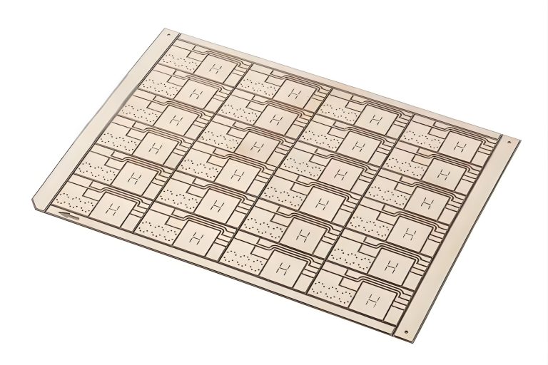
- Industrial applications of glass wafers
- Optoelectronics and communications
Photonics Integrated Circuit (PIC): Glass wafers are used as low-loss optical waveguide substrates for 400G/800G optical modules.
AR/VR optical devices: micro-nano structured glass wafers for making diffraction gratings and waveguides
Lithographic mask: Quartz glass is used for lithographic mask
- MEMS and sensors
Inertial sensor: glass wafer packaged silicon based MEMS structure, resistant to electromagnetic interference.
Microfluidic chips: used for biological detection, the chemical inertness of glass avoids sample contamination.
Pressure sensor: the low expansion coefficient of glass and silicon is used to reduce temperature drift
Gyroscope: Glass wafer used as the structural layer of MEMS gyroscope
- Display technology
OLED/LCD backplane: high flatness glass wafer supports TFT array to improve display uniformity.
MINI/MICRO LED: Temporary bonded glass carrier (CARRIER GLASS), solving the problem of massive transfer.
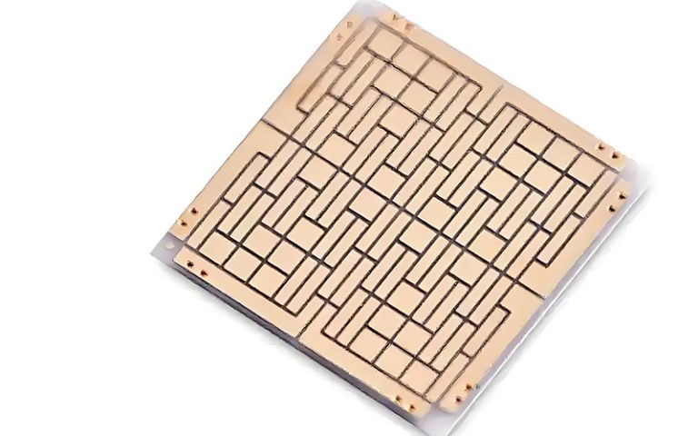
- Advanced packaging
2.5D/3D packaging interposer: Glass through-hole (TGV) technology enables high density interconnection with 30% lower signal loss than silicon through-hole (TSV)
- Power electronic devices
Insulating substrate: as a heat dissipation substrate in IGBT module, it replaces ceramic (such as AL₂O₃) and has both high thermal conductivity (1.4 W/ (M·K)) and insulation.
High voltage isolation: insulation support for power electronic equipment, withstand voltage> 10 KV.
- Technical index advantages of glass wafers
- Insulation and reliability: high resistivity and voltage resistance, avoid leakage of devices, improve system stability.
- High temperature process compatibility: can withstand more than 1000℃ processing, suitable for semiconductor processes requiring high temperature annealing.
- Optical integration advantages: transparency and low refractive index support the on-chip integration of optoelectronic devices.
- Cost and scale: The mass production technology of synthetic quartz glass is mature, and the cost is lower than that of single crystal materials such as sapphire.
- Future development trends
- Process bottleneck: The depth to width ratio of glass through-hole (TGV) needs to be broken through 20:1 (currently about 10:1) to support more dense interconnection.
- Market growth: The global glass wafer market is expected to reach $4.7 billion in 2028, CAGR 8.5%, driven by AI chip packaging and optical communication.
- Technology integration: develop high temperature power devices with silicon carbide (SIC), or achieve flexible glass substrate with polymer composites
Glass wafers, with their unique optical, thermal, and mechanical properties, are penetrating from traditional display applications into high-end semiconductor uses such as photonic chips and advanced packaging. As TGV technology and nanoimprint processes mature, their advantages of being “transparent, insulating, and functional” will be further realized, making them one of the core materials for next-generation heterogeneous integration technologies.


