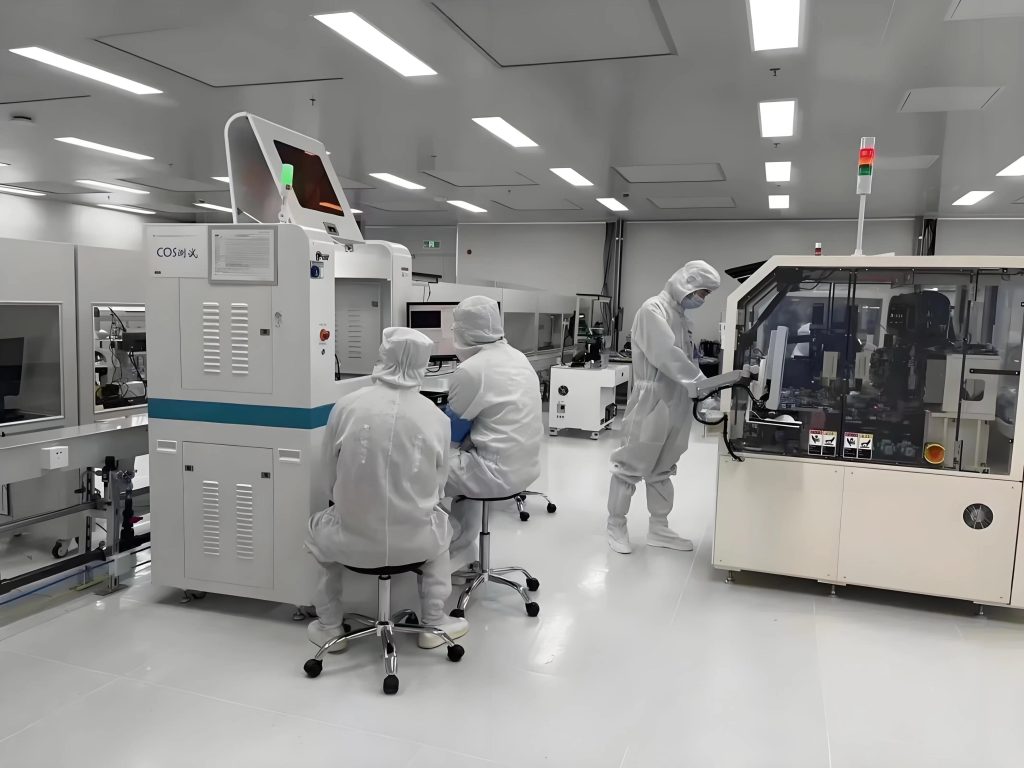
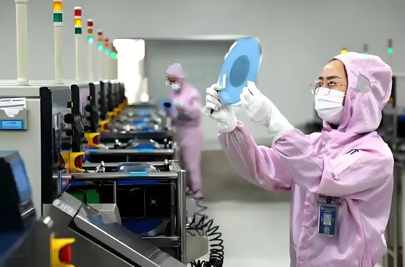
- The manufacturing process of germanium materials
As an IV semiconductor, the manufacturing of germanium needs to take into account ultra-high purity control and crystal integrity optimization. The core process iteration is as follows:
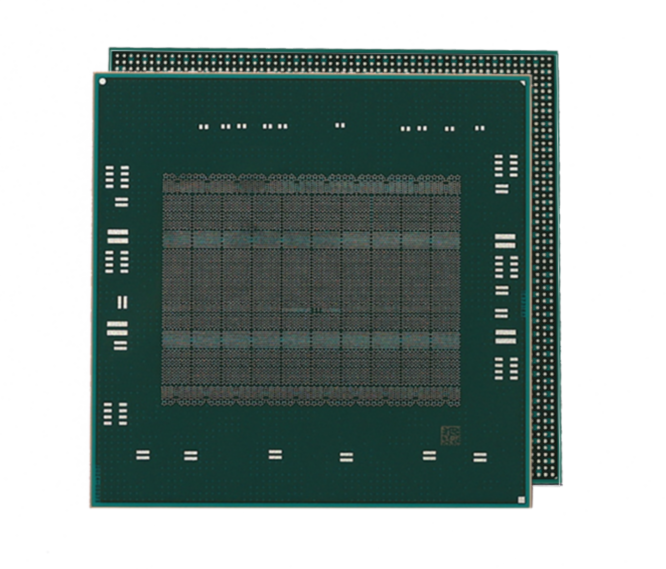
- Preparation of ultra-high purity germanium ingot
Zone melting purification technology: High purity germanium ore (such as germanium stone) is used as the main raw material, and the purity is usually required to be greater than or equal to 99.999%. Electron beam suspension zone melting (EB-FZ) technology is used to melt industrial grade germanium (99.99%) more than 10 times, and the impurity content is reduced to PPB level (phosphorus <5 PPB, boron <2 PPB), and the resistivity is increased to 47 Ω·CM.
Chemical vapor deposition (CVD) purification: GeCL₄ is used as raw material, and germanium film is deposited at 1000℃ through hydrogen reduction reaction to achieve carbon content <1×10¹⁶ CM⁻³.
- Breakthrough in crystal growth technology
Direct pulling (CZ) single crystal growth: using magnetic field direct pulling (MCZ) technology, germanium single crystal with a diameter of 300 MM is grown under argon protection, the dislocation density is less than 5×10³ CM⁻², and the oxygen content is controlled below 1×10¹⁷ CM⁻³.
Vertical gradient solidification (VGF) method: suitable for large size germanium single crystal growth, by optimizing the temperature gradient (5℃/CM) and pulling speed (0.5 MM/H), to obtain a 6-inch germanium substrate with low dislocation density (<1×10⁴ CM⁻²).
- Extension and heterostructure construction
Molecular beam epitaxy (MBE): Ge film is grown at 550℃, with surface roughness <0.5 NM. P-type (BF₃) and N-type (SB) doping concentrations of 10¹⁸-10¹⁹ CM⁻³ are achieved by in-situ doping.
Ge silicon (GESI) strain engineering: by adjusting the SI content (5%-30%), GESI layer was epitaxially grown on the germanium substrate to introduce compressive strain and improve the hole mobility to 1200 CM²/V·S (SI content 15%).
- Advanced post-processing process
Plasma etching: SF₆/O₂ mixed gas plasma is used to achieve high selective etching of germanium nanowires (diameter 50 NM) (germanium: silica = 50:1).
Atomic layer deposition (ALD) passivation: A double layer of AL₂O₃/SINX is deposited on the germanium surface, and the interface state density is reduced to 5×10¹⁰ CM⁻²·EV⁻¹, which improves the reliability of the device.
- Doping and modification
N-type doping: phosphorus (P) or arsenic (AS) is added to increase carrier concentration and optimize conductivity.
Type P doping: boron (B) or aluminum (AL) is added, but lattice integrity must be balanced.
- Material properties and industrial applications of germanium materials
Ge, with its unique physical properties (electron mobility of 3900 CM²/V·S is 2.5 times that of silicon, band gap of 0.67EV), is not as efficient as direct band gap materials, but can enhance light absorption through heterostructure (such as GE/SI) for near-infrared detectors, forming technical barriers in the following fields:
- Infrared optical applications
Thermal imaging detector: Germanium single crystal is used as infrared window material, with transmittance>90% in the 2-14 ΜM band. It is the core material of infrared thermal imaging and night vision equipment. Combined with micro radiometric technology, NETD (noise equivalent temperature difference) <20 MK can be achieved.
Fiber optic communication: The gain coefficient of germanium doped fiber is 15 DB/M at the wavelength of 1550 NM, which is used for long-distance optical signal amplification.
- Efficient solar cells
Three-layer laminated cell: GE (0.66 EV)/GAAS (1.42 EV)/INGAP (1.85 EV) structure with laboratory efficiency of 46% for satellite and space photovoltaic applications.
Perovskite/germanium heterojunction: through interface engineering optimization, the open circuit voltage is 1.25V, the filling factor is 82%, and the photoelectric conversion efficiency is 28.7%.
- High-speed semiconductor applications
Gerbium-based HEMT transistor: The cutoff frequency (Fₜ) of INALAS/INGAAS/GE structure at 300 GHZ is up to 450 GHZ, which is better than that of silicon-based devices.
Gallium quantum dot laser: continuous laser at room temperature at 1.3 ΜM wavelength, threshold current density <100 A/CM², for data center optical interconnection.
High thermal conductivity (60 W/M·K): better than silicon (150 W/M·K) but lower than gallium arsenide (46 W/M·K), suitable for power devices in high temperature environment
- Quantum information technology
Vacancy color center in germanium: vacancy defects are introduced into germanium by electron irradiation to achieve 540 NM single photon emission (purity>98%), which is used for quantum key distribution.
Germanium-based quantum dots: A germanium quantum dot single photon source compatible with silicon, with a repetition frequency of up to 2 GHZ, suitable for on-chip quantum computing.
- Flexible electronics and sensors
Germanium nanowire sensor: Germanium nanowire with a diameter of 20 NM has a sensitivity of 10⁴ PPM⁻¹ to NO₂ gas and a response time of less than 10 S for wearable air quality monitoring.
Flexible germanium transistor: A germanium thin film transistor prepared on a polyimide substrate, with a bending radius of 5 MM, has a mobility of more than 80%, which is suitable for flexible display drive circuit.
- Radiation detection and medicine
High purity germanium detector: used for nuclear radiation monitoring and medical imaging (such as PET scanning), energy resolution of 0.1%, far superior to silicon detector.
Biosensor: After modification of germanium nanowire, DNA/protein can be detected with sensitivity up to femmol level, which can be used for precision medicine
- Third, technology comparison and future trends| key index | Gallium (2025) | silicon (SI) | Gallium arsenide (GAAS)| Electron mobility (CM²/V·S) | 3900 |1500 CM²/VS | 8500| band gap (EV) | 0.66 | 1.12 | 1.42| Infrared response wavelength | COSMO (2-14 ΜM) | Visible (0.4-1.1 ΜM) | Near infrared (0.8-1.7 ΜM)| Thermal conductivity (W/M·K) | 60 | 148 | 46| Integration density (device/CM²) | 1×10⁶ | 5×10⁶ | 2×10⁶
| High frequency application limit | Millimeter wave (30-300 GHZ) | Microwave (<100 GHZ) | Millimeter wave (above 60 GHZ)
- Industry ecology caseMilitary: Lockheed Martin has used germanium infrared Windows to increase the ISTR system detection range of the F-35 fighter to 400 KM.Communication field: Huawei The germanium silicon millimeter wave chip developed supports the 240 GHZ band and is applied to 5G millimeter wave base station.Energy: German FRAUNHOFER Institute has developed a germanium-based laminated solar cell with an efficiency of 44% for high-altitude long-duration missions for drones.Semiconductor devices: Germanium is an important material for manufacturing key components such as transistors and integrated circuits. In high frequency and high speed electronic equipment, germanium is favored for its electron mobilityFuture development trends
- Germanium/2D material heterojunction: Germanium is combined with molybdenum disulfide (MOS₂) to achieve the threshold voltage of 0.1V and the switching ratio of 10⁸ for field-effect transistors, which is suitable for low-power logic circuits.
- Heterogeneous integration technology: heterogeneously integrate germanium with silicon and gallium nitride (GAN) to develop high frequency and high power devices.
- Wafer-scale mass production: optimize CVD and MBE processes, reduce the cost of high purity germanium, and expand the consumer electronics market
- Germanium quantum computing chip: Using spin qubits in germanium, decoherence time> 1 second can be achieved with the help of nuclear spin, promoting the development of fault-tolerant quantum computing.
- Germanium-based optoelectronic integration: Germanium photodetectors and silicon-based electronic circuits are integrated on silicon substrates to realize single-chip optical communication modules with data rates up to 100 GB/S.
- Environmental protection process innovation: develop germanium waste recovery technology, through hydrometallurgy to increase the recovery rate of germanium to 99%, reduce the material cost.
Summary of advantages:
High frequency low noise: Germanium is superior to silicon in millimeter wave band and lower than gallium arsenide in cost.
Infrared compatibility: Wide infrared transmittance makes it irreplaceable in military and medical imaging.
Quantum potential: Germanium quantum dots are compatible with silicon process and are an important direction for future quantum computing
Germanium materials, with their high mobility, low bandgap, and compatibility with silicon processes, hold a critical position in infrared optics, high-efficiency photovoltaics, and quantum technology. In the future, breakthroughs in germanium/2D material heterojunctions and quantum computing could make germanium one of the core materials for next-generation semiconductor technologies, driving revolutionary developments in optoelectronics, information technology, and energy.


