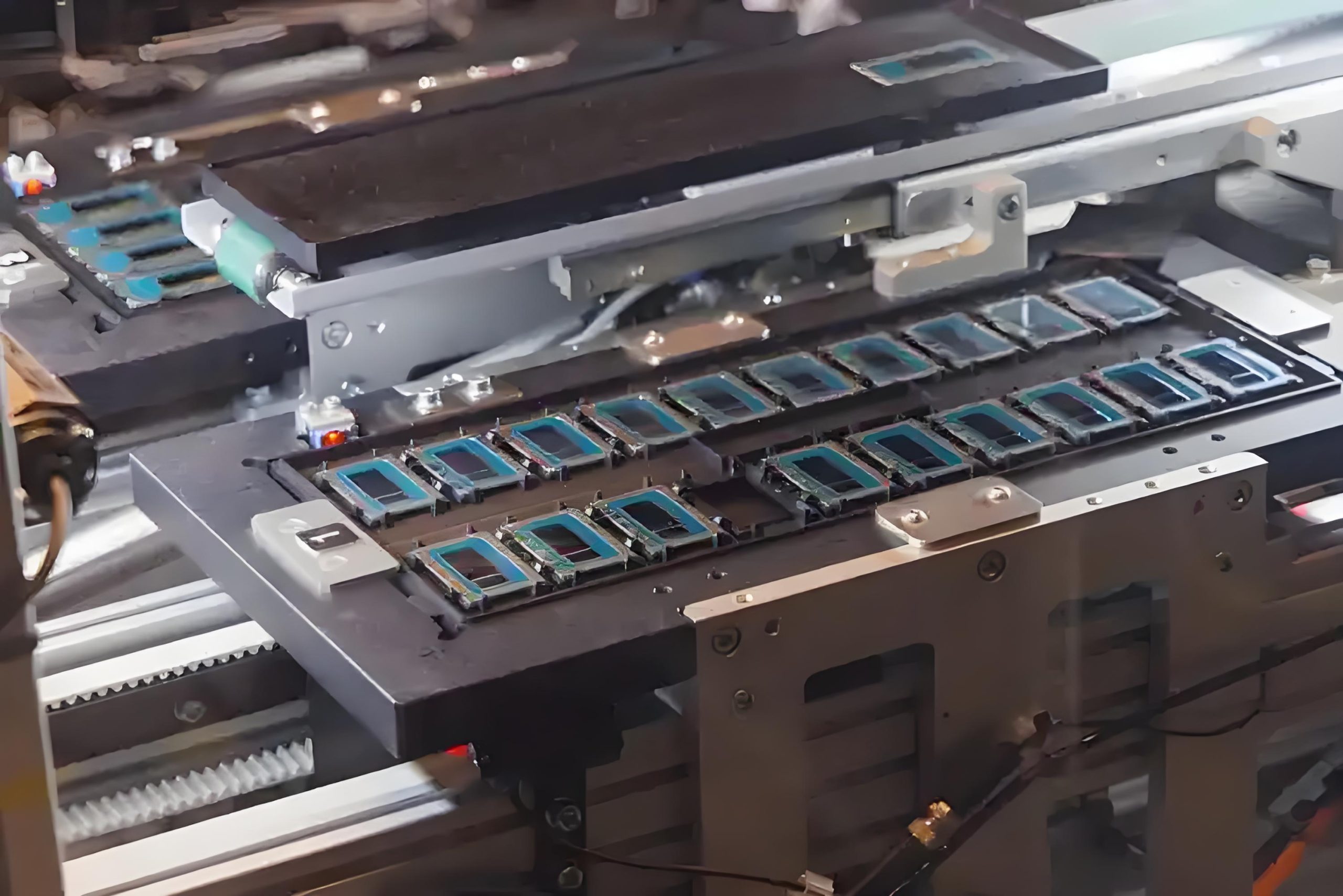
- Ultra-high density interconnection capability
Ball array layout: supports hundreds to thousands of I/O (4002500+ balls), ball spacing can be as low as 0.5MM, far more than traditional QFP packaging.
Short interconnect path: the solder ball directly connects the substrate and PCB, reducing parasitic inductance (<0.1NH) and improving high-speed signal integrity (>10GHZ).
- Excellent thermal management performance
High thermal conductivity ceramic substrate: The thermal conductivity coefficient of ALN substrate is up to 150200 W/M·K, which can be integrated with copper column or metal cover (thermal resistance as low as 28°C/W).
Bottom heat dissipation design: direct heat dissipation through solder balls or metal pads, supporting 50300W high power chips (CPU/GPU).
- Environmental reliability and long life
Air tightness is optional: metal or glass sealed version leakage rate <1 x 10⁻⁸ ATM·CC³/SEC, meeting MILSTD883 standard.
Extreme environment: working temperature 55°C to +200°C, resistant to humidity and heat, salt spray and mechanical impact (vehicle, aerospace applications).
- Mechanical stability
Resistant to deformation: thermal expansion coefficient (CTE) 67 PPM/°C, better compatibility with PCB than plastic BGA, reducing the risk of thermal cycle failure.
- Prominent technical indicators in industrial applications
| qualification | Typical values/characteristics | Application impact
| Number of solder balls / spacing | 4002500+ solder balls, spacing 0.51.27MM | Ultra-high density IC packaging (FPGA, AI acceleration chip)
| Thermal resistance (RTH) | 28°C/W (ALN substrate + copper column heat dissipation) | Supports 200W+ power devices (HPC chips)
| frequency response | DC~40GHZ+ (LTCC optimized design) | 5G millimeter wave, optical communication DSP chip
| Air tightness grade | Optional air tight/non-air tight version | Aerospace/medical needs airtight, consumer electronics can reduce costs
| Mechanical reliability | Drop resistance>5000 cycles (JEDEC) | Vehicle electronics vibration resistance requirements
- The most suitable application scenarios
- High performance computing (HPC) and AI
Server CPU/GPU: Nvidia A100, Intel Xeon processor ceramic heat dissipation optimized version.
FPGA accelerator card: XILINX VERSAL ACAP chip high temperature resistant packaging.
- Communications infrastructure
5G base station AAU: high frequency packaging of millimeter wave RF front end module (28/39GHZ).
Optical module engine: 800G/1.6T Co-packaging of DSP and optical devices for coherent optical communication (CPO).
- Aerospace and defense
Spaceborne computer: long-term reliable packaging of radiation-hardened processors (RISCV architecture).
Electronic warfare system: high frequency signal processing module (X-band radar).
- Automotive electronics (high-end scenario)
Autonomous driving domain controller: thermal solution for high-power chips (NVIDIA THOR).
On-board radar: MMIC package for 4D imaging radar (77GHZ).
- 3D integration and heterogeneous packaging
Silicon interlayer integration: 3D stacking (CPU+HBM memory) is achieved through TSV, with bandwidth>1TB/S.
CHIPLET Technology: Multi-chip CBGA packaging (INTEL EMIB solution) to reduce cost and improve yield.
- High frequency and terahertz adaptation
Ultra-low loss LTCC: Develop glass ceramics with DK <3.5 to support 100GHZ + terahertz communication (6G).
RF optical hybrid integration: the photonic IC is co-packaged with the RF front end (LIDAR).
- Heat dissipation technology revolution
Two-phase microchannel cooling: embedded evaporative cooling, solving the heat flux density>500W/CM².
Diamond substrate: local deposition of diamond (thermal conductivity> 2000 W/M·K) for heat dissipation in hot spots.
- Cost optimization and standardization
Large panel level packaging: 600x600MM² large-scale production of ceramic substrate, cost reduction of more than 30%.
Lead-free solder replacement: Copper column bump (CU PILLAR) replaces tin balls to improve reliability and comply with environmental regulations.
- Expansion of emerging areas
Quantum computing: cryogenic CBGA packaging of superconducting qubit control circuits (<4K).
Space economy: The need for low-cost, highly reliable packaging of giant constellation satellites (KUIPER).
CBGA packaging, with its ultra-high density, superior heat dissipation, and reliability, has become a core solution in HPC, communications, and aerospace. In the future, through the integration of 3D technology, CHIPLET, and advanced thermal management materials, its applications will expand to cutting-edge fields such as terahertz communication and quantum computing. As ceramic substrates achieve large-scale production and design standardization, CBGA is poised to transition from “high-end specialized” to “high-performance universal,” becoming the cornerstone of packaging for next-generation computing and communication equipment.


