Raw materials
High purity alumina (AL₂O₃) is the substrate, and the purity is usually between 90% and 99.9%. Common specifications include 90%,95%,99% and so on. The higher the purity, the better the electrical insulation and thermal conductivity.
Conventional grade: AL₂O₃ content is 92%-96%, and additives such as SIO₂ and MGO are added to optimize sintering performance.
High purity grade: AL₂O₃ content is more than 99%, suitable for high frequency, high temperature and other harsh environment.
- Raw material preparation:
Auxiliary sintering agents: such as silica (SIO₂), magnesium oxide (MGO), etc., are used to improve the sintering performance and mechanical strength, reduce the sintering temperature, promote densification, and refine to sub-micron level through ball milling
Other oxides: such as calcium oxide (CAO), titanium oxide (TIO₂), etc., to adjust the coefficient of thermal expansion or dielectric properties.
Other oxides such as zirconia (ZRO₂), magnesium oxide (MGO), calcium oxide (CAO), strontium oxide (SRO) and titanium dioxide (TIO₂), yttrium oxide (Y₂O₃) can be added to improve the properties of the material.
- Forming process:
Dry pressing: high pressure (50-200 MPA) pressing into the body, suitable for simple shapes.
Flow forming: the paste is formed into a film by flow, and an even sheet is formed by a blade. After drying, it is cut into a substrate for multi-layer circuit substrates, which are used to manufacture ultra-thin substrates (thickness <1MM) suitable for high-density packaging.
Injection molding: the slurry is injected into the mold and solidified by heating.
- Sintering process:
High temperature sintering (1500-1700℃) forms a dense ceramic structure, and atmosphere control (air or inert gas) affects grain size and purity
- reprocessing
Precision processing: grinding and polishing to high precision size (flatness ≤ 10ΜM).
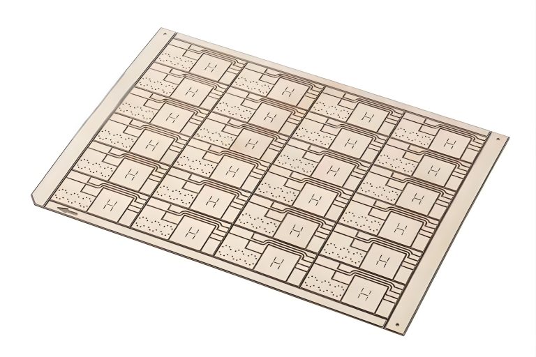
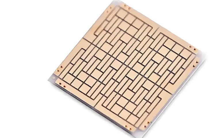
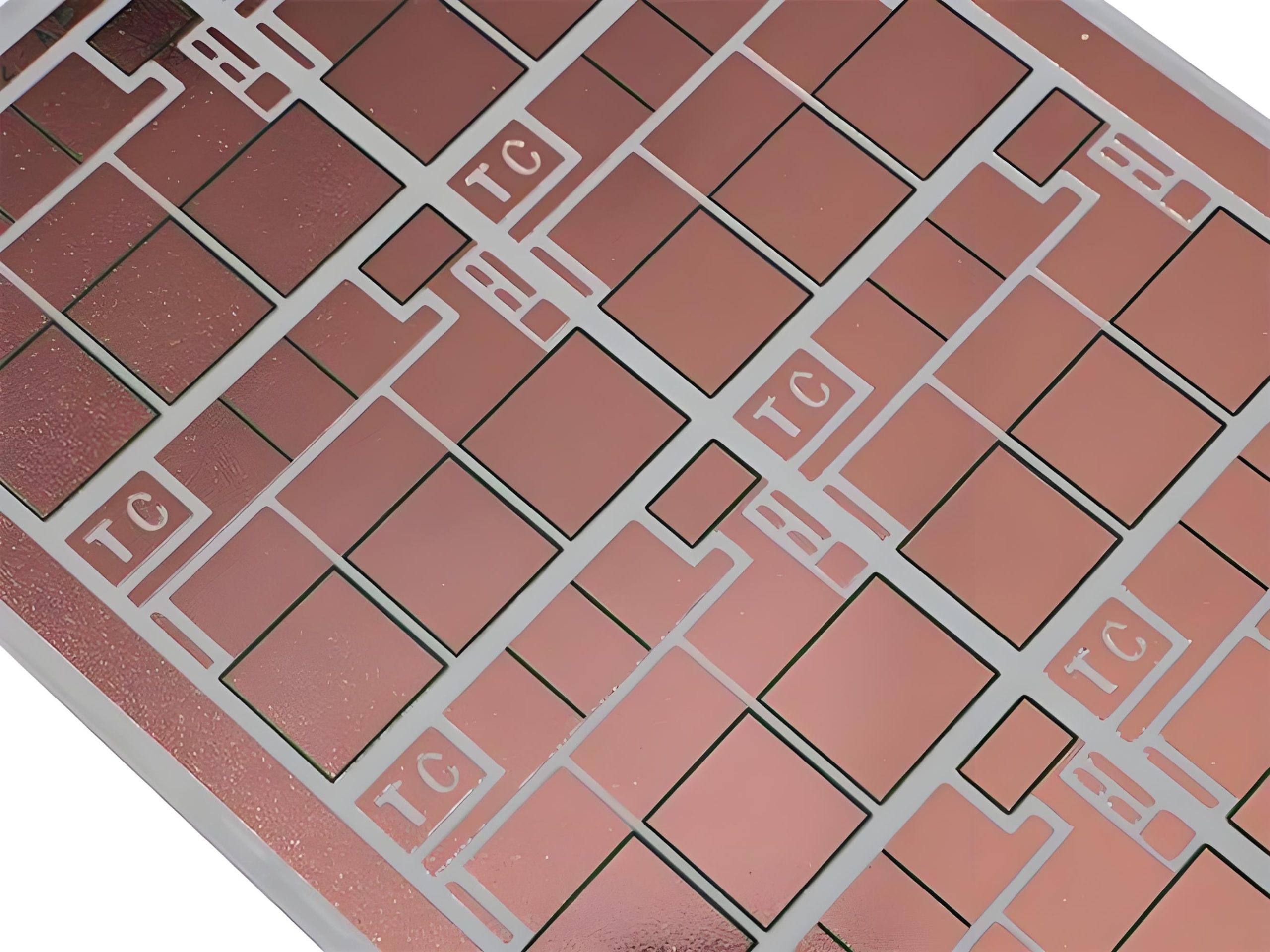
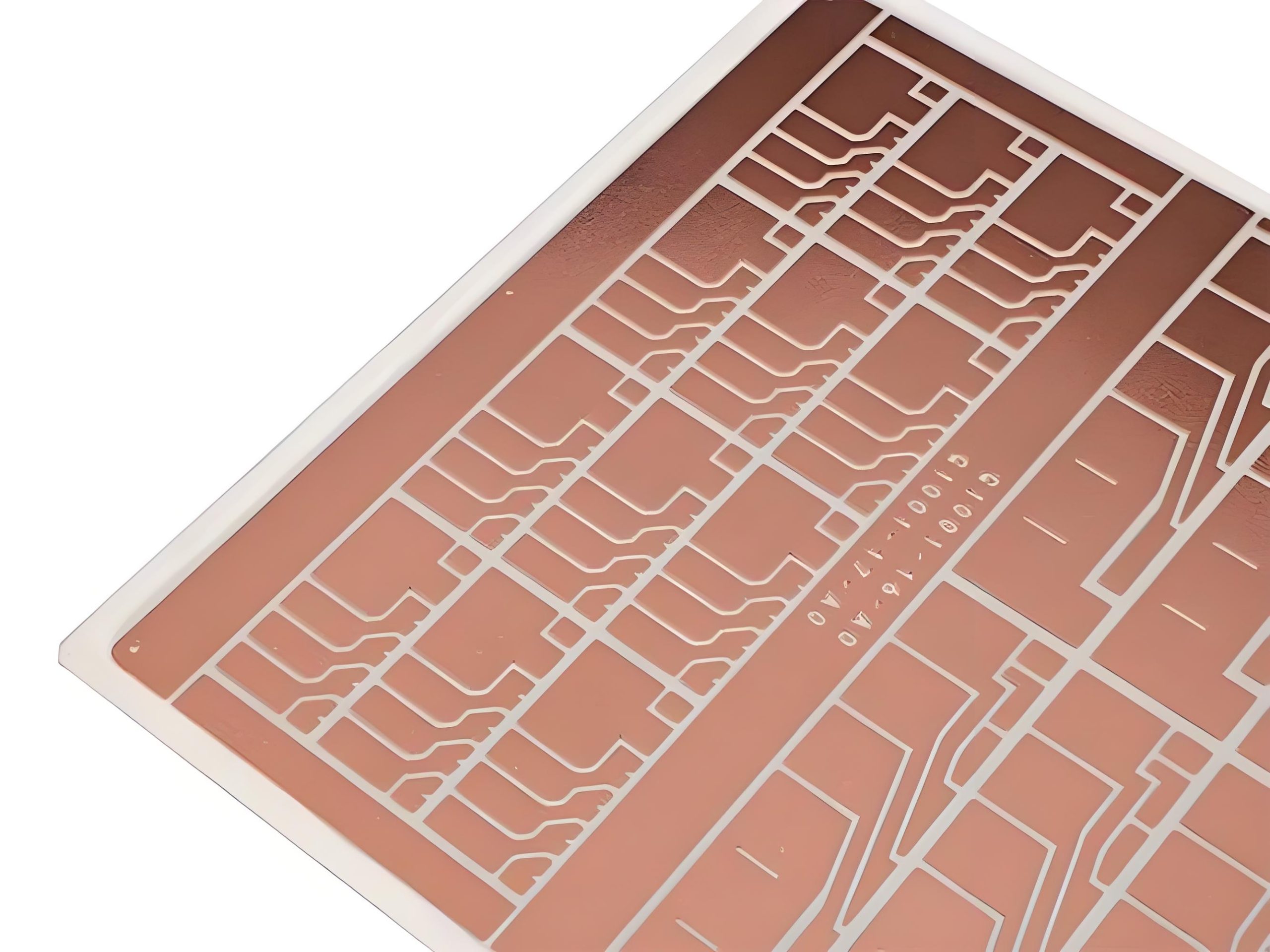
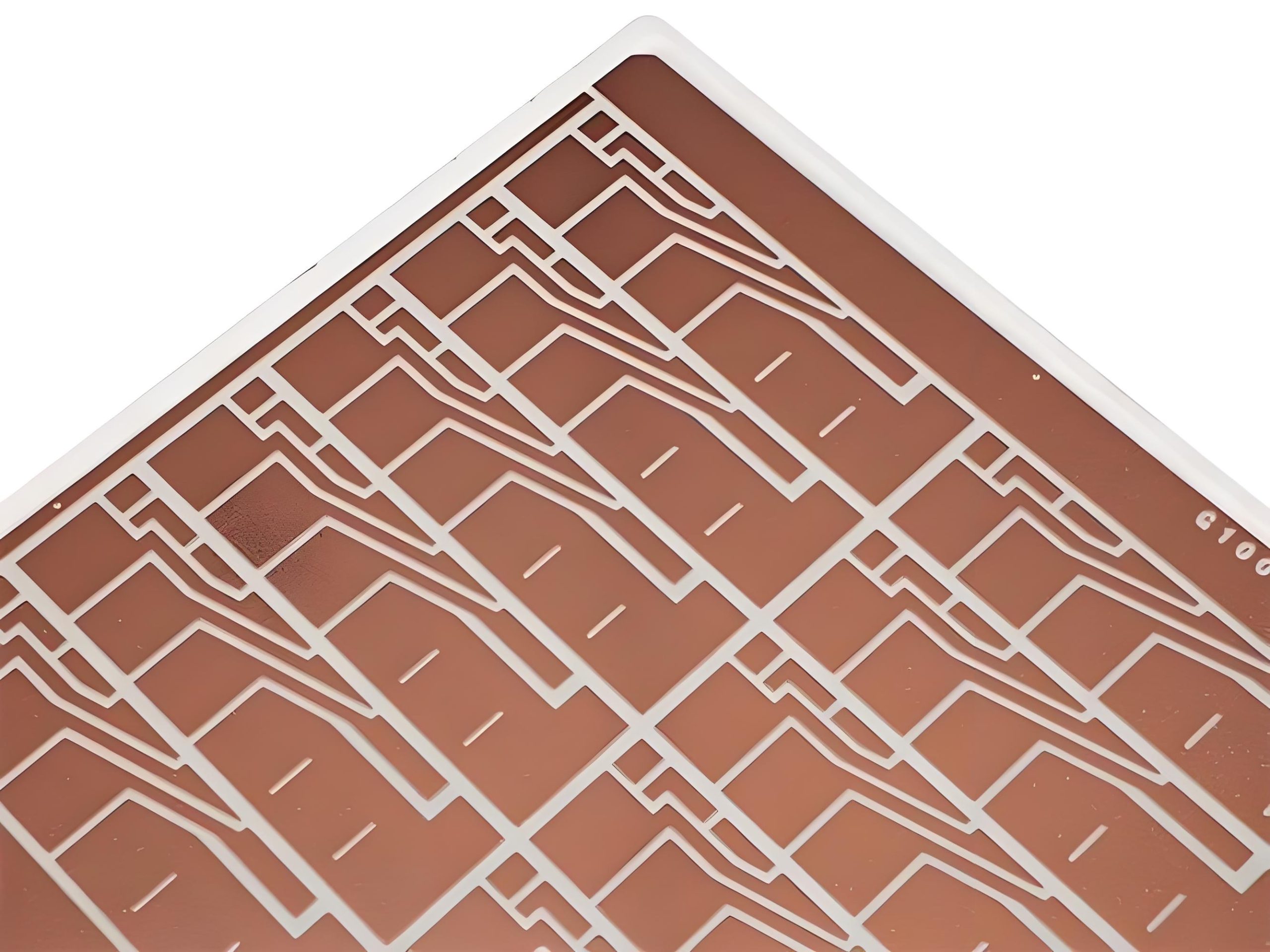
Metallization: circuit connections are achieved by thick film printing (AG/PD paste), sputtering (CU/AL film) or laser activation
- Quality inspection
The thickness uniformity, surface flatness, electrical and thermal properties of the substrate were tested.
- Post-processing:
Laser cutting, drilling, and surface metallization (thick film printing or thin film deposition of CU/AU) form a conductive layer.
| performance index | Values/characteristics | Advantageous scenarios
| heat conductivity | 20-30 W/ (M·K) (95% purity) | Medium and high power heat dissipation
| insulation strength | 10-15 KV/MM High pressure environmental stability
| Thermal expansion coefficient | 6.5-8.5 x 10⁻⁶/℃ | Compatible with SI chips
| mechanical strength | Bending strength 300-400 MPA | Resistance to mechanical stress
| temperature tolerance | Long-term use temperature> 1600℃ | High temperature packaging
| dielectric constant | 9-10(1 MHZ) | Low loss of high frequency signal
| thermostability | 2050℃ (melting point) | Can work for 300℃ for a long time
| resistivity | >10¹⁴ Ω·CM | Low loss of high frequency signal
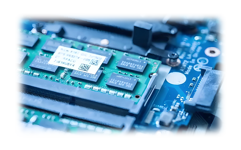
- Power electronics module:
IGBT module: alumina ceramic substrate is used as the insulating substrate of power module to improve heat dissipation performance and reliability.
MOSFET Module: alumina ceramic substrate is used for the packaging of high frequency power devices.
It is superior to FR-4 substrate (thermal conductivity <0.3 W/ (M·K)), supports IGBT/MOSFET heat dissipation, and the operating temperature can reach 300℃.
- LED package:
LED substrate: Alumina ceramic substrate is used for the packaging of LED chips to improve heat dissipation performance and life, which is 50% lower than that of aluminum nitride (thermal conductivity 200+ W/ (M·K)), meeting the needs of general lighting; light efficiency is improved by 15%, and the life is>50,000 hours.
- RF devices:
The dielectric loss (TANΔ<0.0002) is lower than that of plastic substrate and is suitable for 5G millimeter wave band.
- Automotive electronics:
The humidity resistance (85℃/85% RH) test is greater than 1000 hours through the AEC-Q200 certification.
- Aerospace:
Radiation resistance: anti Γ ray> 100 KGY, used in satellite power system.
- Compare other substrate materials
| Material | Thermal conductivity [W/ (M·K)] | Cost | Processing difficulty | Applicable scenarios
| Aluminum oxide ceramics | 20-30 | Low | Medium | Medium power, high frequency, general
| Aluminum nitride ceramics | 150-220 | High | High | High power laser
| Beryllium oxide ceramics | 280 | Very high | Toxic | Military high frequency devices (restricted)
| FR-4 | 0.3 | Very low | Easy | Low power consumption of consumer electronics
- Future development trends
- High performance
Develop high purity (>99.9%) alumina ceramic substrate to improve performance and reliability.
- Thinness
Develop thinner alumina ceramic substrate to improve the integration and heat dissipation performance.
- Multi-functionality
New functions (such as anti-reflection, self-cleaning) are given to the substrate through surface modification or coating process.
- Green manufacturing
Promote the manufacturing process of environmentally friendly alumina ceramics to reduce energy consumption and pollution.
Alumina ceramic substrate occupies a dominant position in the field of semiconductor packaging due to its high cost performance, mature process and balanced comprehensive performance. Its excellent electrical, thermal and mechanical properties are widely used in power modules, LED packaging, sensors and RF devices. With the development of 5G and electric vehicles, its demand will continue to grow.


