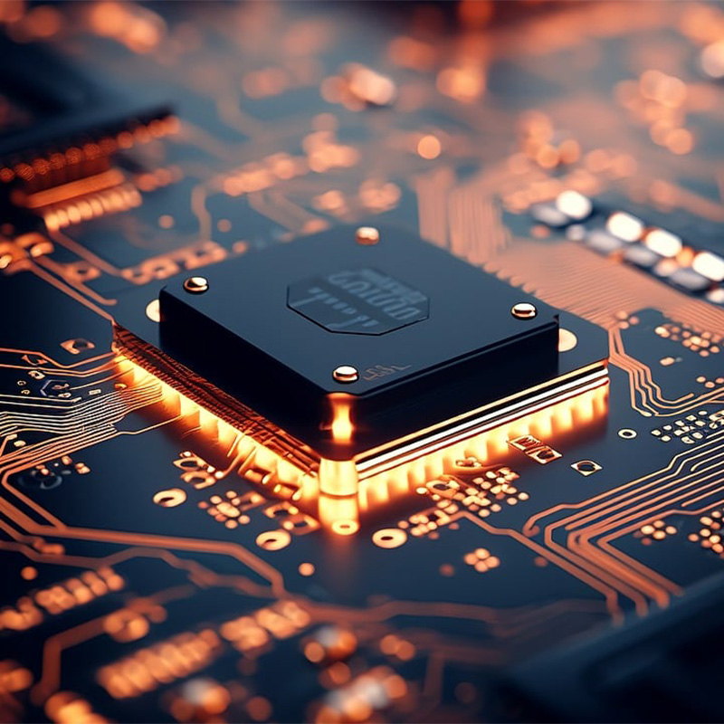
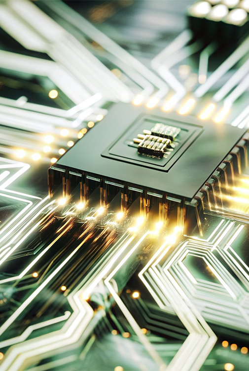
Semiconductor ceramic tubes and ceramic substrates provide key support for AI hardware. The rapid development of artificial intelligence technology has increased the demand for high-performance computing (HPC) systems, data centers, and smart devices, and the demand for high-performance, high-reliability optical modules and other electronic components has also increased.
Helping the AI industry
Airtightness and heat dissipation performance: Ceramic tube shells are widely used in optical modules due to their excellent airtightness, ensuring that internal devices are protected from environmental factors. Especially in liquid-cooled data center environments, airtight packaging methods such as butterfly packaging BOX and coaxial packaging TO-CAN help protect sensitive optoelectronic conversion devices.
Mechanical support and electrical connection: The multi-layer co-fired ceramic insulation structure not only provides physical support for the chip in the optical module, but also serves as an electrical signal transmission channel and optical coupling interface, realizing the interconnection between the chip and the external circuit.
Breakthrough Innovation
Application of new materials:
Application of new materials: Materials such as aluminum nitride (AlN) and beryllium oxide (BeO) are gradually replacing traditional aluminum oxide (Al2O3) due to their good thermal conductivity and electrical insulation properties to meet the heat dissipation needs under higher power density.
High frequency stability:
High frequency stability: Ceramic bases used in quartz crystal oscillators and quartz crystal resonators can precisely control digital signal frequencies and maintain clock synchronization of optical signals, which is critical for high-speed optical modules used in AI servers.
Efficient heat dissipation management:
Efficient heat dissipation management: For high-power optical modules, ceramic heat sinks can effectively conduct the heat generated during operation, maintain a low operating temperature, and thus ensure stable operation of the system.
Breakthrough Innovation
Improved AMB (Active Metal Brazing) Ceramic Substrate Inspection Efficiency:
Improved AMB (Active Metal Brazing) Ceramic Substrate Inspection Efficiency: The new patented AMB ceramic substrate inspection silo technology optimizes the storage and retrieval process through the flip function, improving inspection speed and accuracy.
FCBGA (flip chip ball grid array) packaging substrate: FCBGA packaging substrate provides better electrical performance and heat dissipation capabilities for AI chips, reduces electrical noise and improves signal transmission speed.
02
High surface finish alumina ceramic substrate:
High surface finish alumina ceramic substrate: This material has extremely high surface flatness and cleanliness, which has a direct impact on the yield in the semiconductor manufacturing process. It is especially suitable for AI-related applications that require high-precision processing.